BATTERY PROTECTION IC FOR 1-SERIAL TO 4-SERIAL-CELL PACK (SECONDARY PROTECTION)
Rev.6.1_00
S-8244 Series
Seiko Instruments Inc.
7
Absolute Maximum Ratings
Table 7
(Ta = 25°C unless otherwise specified)
Item Symbol Applied pin Rating Unit
Input voltage between VCC and VSS V
DS
VCC V
SS
0.3 to V
SS
+26 V
Delay capacitor connection pin voltage V
ICT
ICT V
SS
0.3 to V
CC
+0.3 V
Input pin voltage V
IN
SENSE, VC1,
VC2, VC3
V
SS
0.3 to V
CC
+0.3 V
(CMOS output) V
SS
0.3 to V
CC
+0.3 V
(Nch open drain output) V
SS
0.3 to 26 V
CO output pin
voltage
(Pch open drain output)
V
CO
CO
V
CC
26 to V
CC
+0.3 V
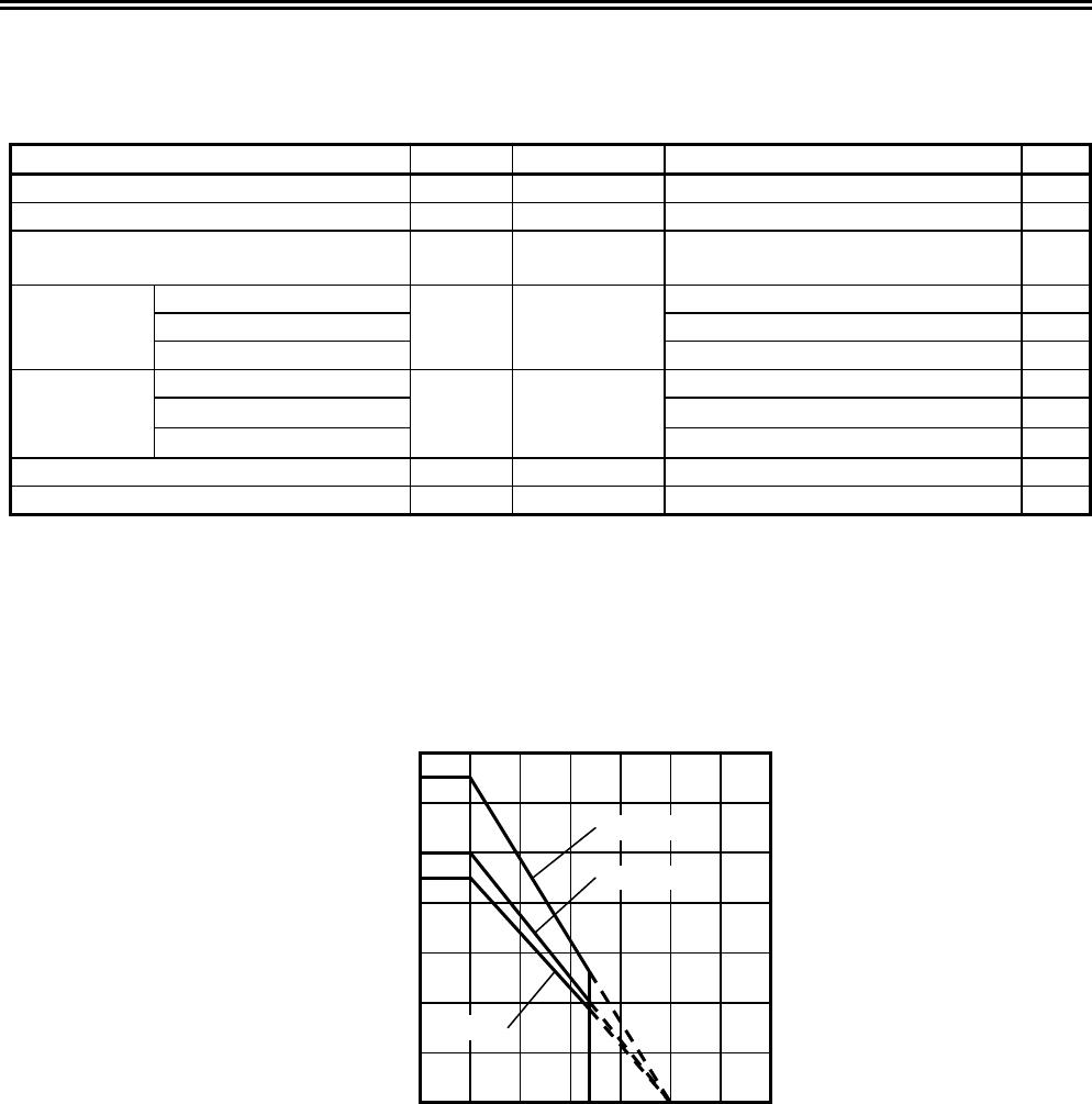
SNT-8A
450
*1
mW
8-Pin MSOP
500
*1
mW
Power
dissipation
TMSOP-8
P
D
650
*1
mW
Operating ambient temperature T
opr
40 to +85 °C
Storage temperature T
stg
40 to +125 °C
*1. When mounted on board
[Mounted board]
(1) Board size : 114.3 mm × 76.2 mm × t1.6 mm
(2) Name : JEDEC STANDARD51-7
Caution The absolute maximum ratings are rated values exceeding which the product could suffer physical
damage. These values must therefore not be exceeded under any conditions.
0 50 100 150
Ambient Temperature (Ta) [°C]
700
600
500
400
300
200
100
0
Power Dissipation (P
D
) [mW]
TMSOP-8
8-Pin MSOP
SNT-8A
Figure 5 Power Dissipation of Package (When Mounted on Board)
BATTERY PROTECTION IC FOR 1-SERIAL TO 4-SERIAL-CELL PACK (SECONDARY PROTECTION)
S-8244 Series
Rev.6.1_00
Seiko Instruments Inc.
8
Electrical Characteristics
Table 8
(Ta = 25 °C unless otherwise specified)
Item
Symbol
Conditions Min. Typ. Max. Unit
Test
conditions
Test circuit
DETECTION VOLTAGE
Overcharge detection voltage 1
*1
V
CU1
3.7 V to 4.5 V Adjustment
V
CU1
0.025
V
CU1
V
CU1
+
0.025
V 1 1
Overcharge detection voltage 2
*1
V
CU2
3.7 V to 4.5 V Adjustment
V
CU2
0.025
V
CU2
V
CU2
+
0.025
V 2 1
Overcharge detection voltage 3
*1
V
CU3
3.7 V to 4.5 V Adjustment
V
CU3
0.025
V
CU3
V
CU3
+
0.025
V 3 1
Overcharge detection voltage 4
*1
V
CU4
3.7 V to 4.5 V Adjustment
V
CU4
0.025
V
CU4
V
CU4
+
0.025
V 4 1
Overcharge hysteresis voltage 1
*2
V
CD1
0.28 0.38 0.48 V 1 1
Overcharge hysteresis voltage 2
*2
V
CD2
0.28 0.38 0.48 V 2 1
Overcharge hysteresis voltage 3
*2
V
CD3
0.28 0.38 0.48 V 3 1
Overcharge hysteresis voltage 4
*2
V
CD4
0.28 0.38 0.48 V 4 1
Detection voltage
temperature coefficient
*3
T
COE
Ta =
40
°
C to
+
85
°
C
*4
0.4 0.0
+
0.4 mV/
°
C
DELAY TIME
Overcharge detection delay time
t
CU
C = 0.1
μ
F 1.0 1.5 2.0 s 5 2
OPERATING VOLTAGE
Operating voltage
between VCC and VSS
*5
V
DSOP
3.6
24 V
CURRENT CONSUMPTION
Current consumption
during normal operation
I
OPE
V1 = V2 = V3 = V4 = 3.5 V
1.5 3.0
μ
A 6 3
Current consumption at
power down
I
PDN
V1 = V2 = V3 = V4 = 2.3 V
1.2 2.4
μ
A 6 3
VC1 sink current
I
VC1
V1 = V2 = V3 = V4 = 3.5 V
0.3
0.3
μ
A 6 3
VC2 sink current
I
VC2
V1 = V2 = V3 = V4 = 3.5 V
0.3
0.3
μ
A 6 3
VC3 sink current
I
VC3
V1 = V2 = V3 = V4 = 3.5 V
0.3
0.3
μ
A 6 3
OUTPUT VOLTAGE
*6
CO “H” voltage
V
CO(H)
at I
OUT
= 10
μ
A
V
CC
0.05
V 7 4
CO “L” voltage
V
CO(L)
at I
OUT
= 10
μ
A
V
SS
+
0.05
V 7 4
*1. ± 50 mV when Ta = 40°C to +85°C.
*2. 0.25 ± 0.07 V, 0.13 ± 0.04 V, 0.045 ± 0.02 V except for 0.38 V hysteresis models.
*3. Overcharge detection voltage or overcharge hysteresis voltage.
*4. Since products are not screened at high and low temperature, the specification for this temperature range is guaranteed
by design, not tested in production.
*5.
After detecting the overcharge, the delay circuit operates normally in the range of operating voltage.
*6. Output logic and CMOS or open drain output can be selected.
BATTERY PROTECTION IC FOR 1-SERIAL TO 4-SERIAL-CELL PACK (SECONDARY PROTECTION)
Rev.6.1_00
S-8244 Series
Seiko Instruments Inc.
9
Test Circuits
(1) Test Condition 1, Test Circuit 1
Set switches 1 and 2 to OFF for CMOS output product.
Set switch 1 to ON and switch 2 to OFF for Nch open drain product.
Set switch 1 to OFF and switch 2 to ON for Pch open drain product.
Product with CMOS output active “H”, Nch open drain output active “H”
The overcharge detection voltage 1 (V
CU1
) is a voltage at V1; when the CO pin’s voltage is set to “H” by increasing
V1 gradually, after setting V1 = V2 = V3 = V4 = 3.5 V. After that, gradually decreasing V1’s voltage to set CO = “L”,
and the difference of this V1’s voltage and V
CU1
is the overcharge hysteresis voltage 1 (V
CD1
).
Product with CMOS output active “L”, Nch open drain output active “L”, Pch open drain output active “L”
The overcharge detection voltage 1 (V
CU1
) is a voltage at V1; when the CO pin’s voltage is set to “L” by increasing
V1 gradually, after setting V1 = V2 = V3 = V4 = 3.5 V. After that, gradually decreasing V1’s voltage to set CO =
“H”, and the difference of this V1’s voltage and V
CU1
is the overcharge hysteresis voltage 1 (V
CD1
).
(2) Test Condition 2, Test Circuit 1
Set switches 1 and 2 to OFF for CMOS output product.
Set switch 1 to ON and switch 2 to OFF for Nch open drain product.
Set switch 1 to OFF and switch 2 to ON for Pch open drain product.
Product with CMOS output active “H”, Nch open drain output active “H”
The overcharge detection voltage 2 (V
CU2
) is a voltage at V2; when the CO pin’s voltage is set to “H” by increasing
V2 gradually, after setting V1 = V2 = V3 = V4 = 3.5 V. After that, gradually decreasing V2’s voltage to set CO = “L”,
and the difference of this V2’s voltage and V
CU2
is the overcharge hysteresis voltage 2 (V
CD2
).
Product with CMOS output active “L”, Nch open drain output active “L”, Pch open drain output active “L”
The overcharge detection voltage 2 (V
CU2
) is a voltage at V2; when the CO pin’s voltage is set to “L” by increasing
V2 gradually, after setting V1 = V2 = V3 = V4 = 3.5 V. After that, gradually decreasing V2’s voltage to set CO =
“H”, and the difference of this V2’s voltage and V
CU2
is the overcharge hysteresis voltage 2 (V
CD2
).
(3) Test Condition 3, Test Circuit 1
Set switches 1 and 2 to OFF for CMOS output product.
Set switch 1 to ON and switch 2 to OFF for Nch open drain product.
Set switch 1 to OFF and switch 2 to ON for Pch open drain product.
Product with CMOS output active “H”, Nch open drain output active “H”
The overcharge detection voltage 3 (V
CU3
) is a voltage at V3; when the CO pin’s voltage is set to “H” by increasing
V3 gradually, after setting V1 = V2 = V3 = V4 = 3.5 V. After that, gradually decreasing V3’s voltage to set CO = “L”,
and the difference of this V3’s voltage and V
CU3
is the overcharge hysteresis voltage 3 (V
CD3
).
Product with CMOS output active “L”, Nch open drain output active “L”, Pch open drain output active “L”
The overcharge detection voltage 3 (V
CU3
) is a voltage at V3; when the CO pin’s voltage is set to “L” by increasing
V3 gradually, after setting V1 = V2 = V3 = V4 = 3.5 V. After that, gradually decreasing V3’s voltage to set CO =
“H”, and the difference of this V3’s voltage and V
CU3
is the overcharge hysteresis voltage 3 (V
CD3
).
S-8244AAUFN-CEUT2U

Mfr. #:
Manufacturer:
ABLIC
Description:
Battery Management Li-Ion battery 2nd protection
Lifecycle:
New from this manufacturer.
Delivery:
DHL FedEx Ups TNT EMS
Payment:
T/T Paypal Visa MoneyGram Western Union