11
LT1394
APPLICATIONS INFORMATION
WUU
U
correct, amplified composite signal at the LT1394’s posi-
tive input in Trace D. The LT1394’s output is Trace E. Figure
9 details circuit propagation delay. The output responds in
18ns to a 500µV overdrive on a 1mV step. Figure 10 plots
response time versus overdrive. As might be expected,
propagation delay decreases at higher overdrives. A1’s
noise limits usable sensitivity.
A1 has poorly defined DC characteristics, necessitating
some form of DC correction. A2 and A3, operating at a
differential gain of 100, provide this function. They differ-
entially sense a band limited version of A1’s inputs and feed
DC and low frequency amplified information to the com-
parator. The low frequency roll-off of A1’s signal path
complements A2-A3’s high frequency roll-off. The sum-
mation of these two signal channels at the LT1394 inputs
results in flat response from DC to high frequency.
Figure 8 shows waveforms for the high gain comparator.
Trace A is a 500µV overdrive on a 1mV step applied to the
circuit’s positive input (negative input grounded). Trace B
shows the resulting amplified step at A1’s positive output.
Trace C is A2’s band limited output. A1’s wideband output
combines with A2’s DC corrected information to yield the
5µs/DIV 1394 F08
A = 1mV/DIV
10ns/DIV 1394 F09
A = 1mV/DIV
B = 1V/DIV
B = 0.1V/DIV
(AC-COUPLED)
C = 0.1V/DIV
D = 0.1V/DIV
E = 5V/DIV
Figure 8. 500µV Input (Trace A) Is Split into Wideband
and Low Frequency Gain Paths (Traces B and C) and
Recombined (Trace D). Comparator Output Is Trace E
Figure 9. Parallel Path Comparator Shows 18ns
Response (Trace B) to 500µV Overdrive (Trace A)
RESPONSE TIME (ns)
15
OVERDRIVE (µV)
1100
1000
900
800
700
600
500
16 17 18
1394 F10
Figure 10. Response Time vs Overdrive for the
Composite Comparator
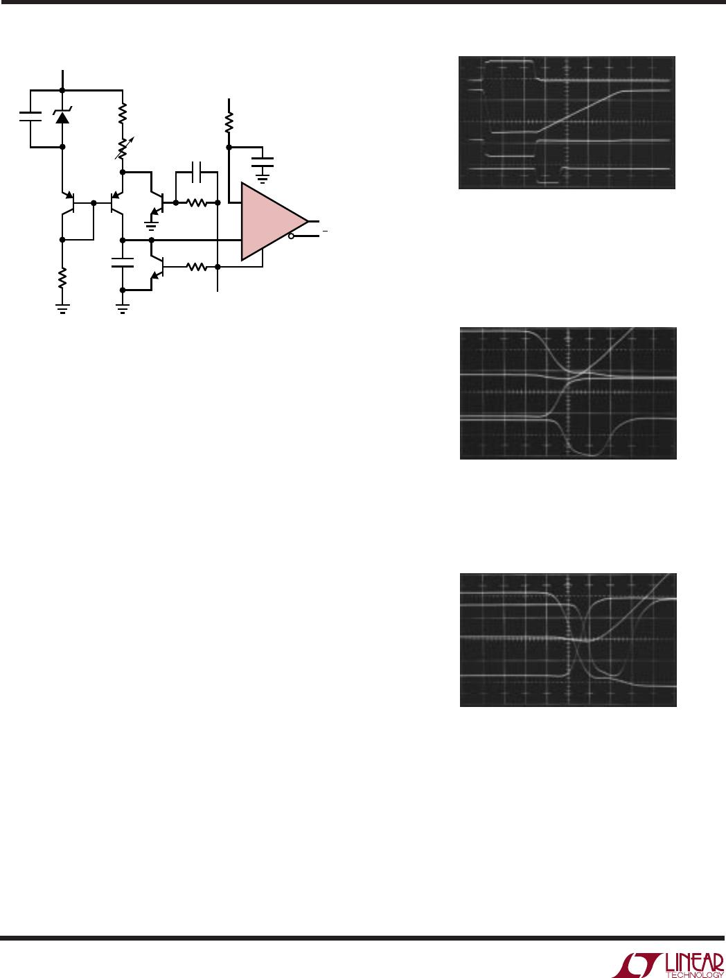
Voltage-Controlled Delay
The ability to set a precise, predictable delay has broad
application in pulse circuitry. Figure 11’s configuration
sets a 0 to 300ns delay from a corresponding 0V to 3V
control voltage. It takes advantage of the LT1394’s speed
and the clean dynamics of an emitter switched current
source.
Q1 and Q2 form a current source that charges the 1000pF
capacitor. When the trigger input is high (Trace A, Figure
12) both Q3 and Q4 are on. The current source is off and
Q2’s collector (Trace B) is at ground. The latch input at the
LT1394 prevents it from responding and its output remains
high. When the trigger input goes low, the LT1394’s latch
input is disabled and its output drops low. Q4’s collector
(Trace C) lifts and Q2 comes on, delivering constant
current to the 1000pF capacitor (Trace B). The resulting
linear ramp at the LT1394’s positive input is compared to
the delay programming voltage input. When a crossing
occurs, the comparator goes high (Trace D). The length of
time the comparator was low is directly proportional to the