13
LT1394
Fast, High Impedance, Variable Threshold Trigger
A frequent requirement in instrumentation is a fast trigger
with a variable threshold. Often, a high impedance input is
also required. Figure 15 meets these requirements. Com-
parator C1 is the basic trigger, with threshold voltage set at
its negative input. Source follower Q1 provides high
impedance with about 2pF input capacitance and 50pA bias
current. Normally, Q1’s source bias point would be uncer-
tain and drifty, but stabilization techniques eliminate this
concern. A1 measures filtered versions of Q1’s gate and
source voltages. A1’s output biases Q2, forcing Q1’s
channel current to whatever value is required to equalize
A1’s inputs, and hence Q1’s gate and source voltages. A1’s
input filtering and roll-off are far slower than input frequen-
cies of interest; its action does not interfere with the
circuit’s main signal path. The 330pF capacitor prevents
fast edges coupled through Q2’s collector base junction
from influencing A1’s operation.
APPLICATIONS INFORMATION
WUU
U
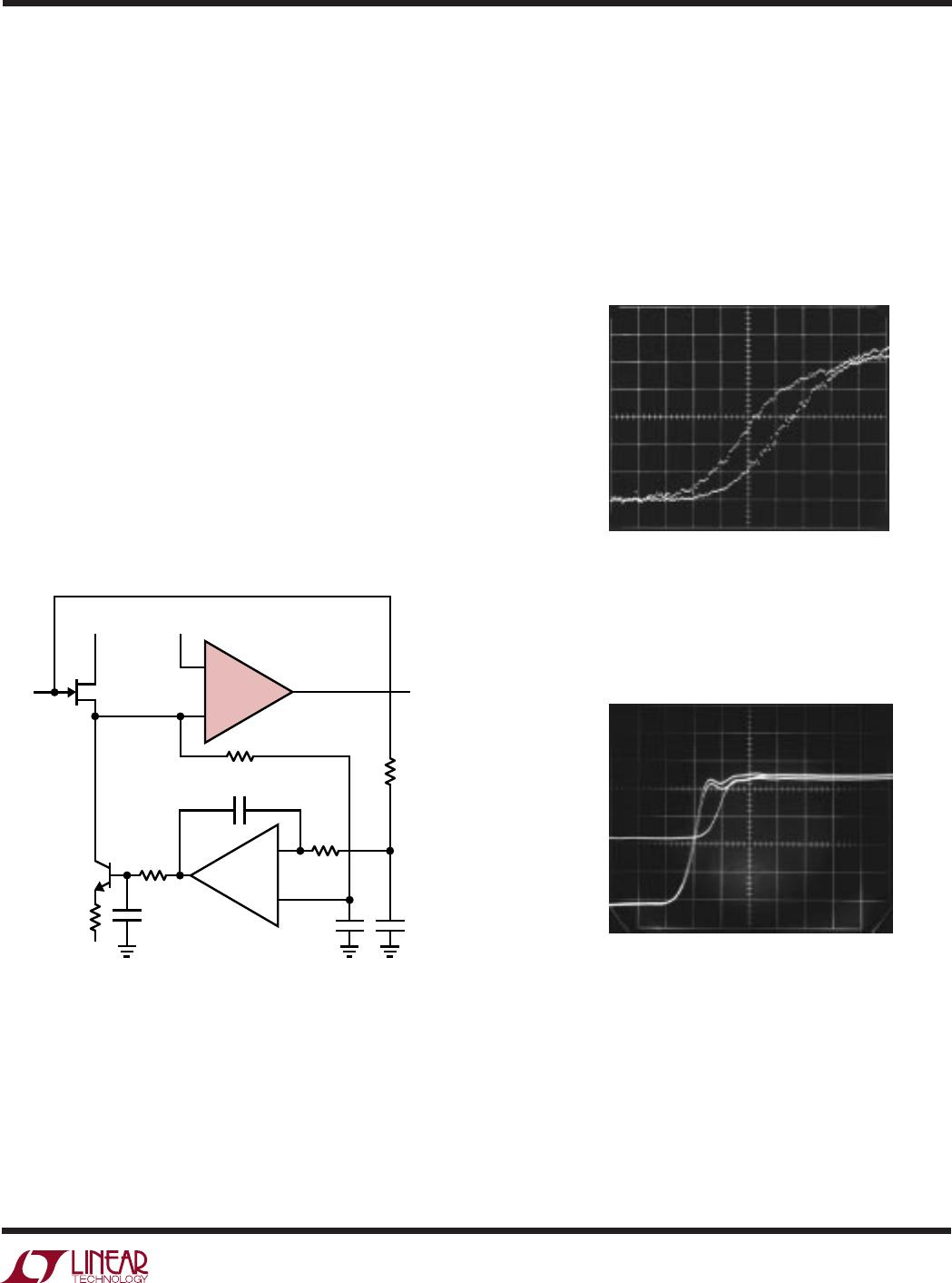
Q1 should contribute negligible timing error to minimize
overall delay. Figure 16’s photo verifies Q1’s wideband
operation. Trace B, Q1’s source, lags the input (Trace A) by
only 300ps. Input, FET buffer output and C1 output appear
as Traces A, B and C, respectively in Figure 17. As before,
the FET buffer is seen to contribute small timing error, and
C1’s output is about 8ns delayed from the input.
+
C1
LT1394
+
A1
LT1097
10M
5V
V
TRIG
±3V
0.01µF
0.1µF
OUTPUT
1394 F15
10k
Q2
2N3904
INPUT
±3V
Q1
2N5486
1.5k
–5V
0.1µF
10M
100
330pF
Figure 15. Buffer Provides 2pF, 50pA Input Characteristics for
Fast Trigger. Amplifier-Stabilized Biasing Eliminates FET Offset
200ps/DIV 1394 F16
Figure 16. Trigger Buffer’s 300ps Delay Minimizes
Timing Error. 4GHz Sampling Oscilloscope’s Output Is
a Series of Dots
A = 1V/DIV
B = 1V/DIV
Figure 17. Input (Trace A), FET Source (Trace B)
and Output (Trace C) Waveforms for the Trigger.
Total Delay Is 8ns
10ns/DIV 1394 F17
A = 1V/DIV
B = 1V/DIV
C = 2V/DIV
14
LT1394
High Speed Adaptive Trigger Circuit
Line and fibre-optic receivers often require an adaptive
trigger to compensate for variations in signal amplitude
and DC offsets. The circuit in Figure 18 triggers on 2mV to
175mV signals from 100Hz to 45MHz while operating from
a single 5V rail. A1, operating at a gain of 15, provides
wideband AC gain. The output of this stage biases a 2-way
peak detector (Q1 through Q4). The maximum peak is
stored in Q2’s emitter capacitor, while the minimum excur-
sion is retained in Q4’s emitter capacitor. The DC value of
the midpoint of A1’s output signal appears at the junction
of the 500pF capacitor and the 3M units. This point
always sits midway between the signal’s excursions,
egardless of absolute amplitude. This signal-adaptive volt-
age is buffered by A2 to set the trigger voltage at the
LT1394’s positive input. The LT1394’s negative input is
biased directly from A1’s output. The LT1394’s output, the
circuit’s output, is unaffected by >85:1 signal amplitude
variations. Bandwidth limiting in A1 does not affect trigger-
ing because the adaptive trigger threshold varies
ratiometrically to maintain circuit output.
APPLICATIONS INFORMATION
WUU
U
Figure 19 shows operating waveforms at 45MHz. Trace A’s
input produces Trace B’s amplified output at A1. The
comparator’s output is Trace C.
Split supply versions of this circuit can achieve band-
widths to 50MHz with wider input operating range.
A = 0.1V/DIV
B = 0.1V/DIV
C = 5V/DIV
50ns/DIV
AN72 F64
Figure 19. Adaptive Trigger Responding to a 40MHz,
5mV Input. Input Amplitude Variations from 2mV to
175mV Are Accommodated
5V
+
A1
LT1227
+
A2
LT1006
INPUT
5V
5V
5V
TRIGGER
OUT
1394 F18
500pF
0.1µF
510
470
470
750
36
1
3
2
4
14
13
15
5
6
12
10
11
2k
10µF
2k
2k
+
0.1µF
0.1µF
0.005µF
0.005µF
100µF
+
Q1, Q2, Q3, Q4 = CA3096 ARRAY:
TIE SUBSTRATE (PIN 16) TO GROUND
= 1N4148
+
LT1394
Q1 Q2
Q3
Q4
3M
3M
Figure 18. 45MHz Single Supply Adaptive Trigger. Output Comparator’s
Threshold Varies Ratiometrically with Input Amplitude, Maintaining Data
Integrity over >85:1 Input Amplitude Range
15
LT1394
Information furnished by Linear Technology Corporation is believed to be accurate and reliable.
However, no responsibility is assumed for its use. Linear Technology Corporation makes no represen-
tation that the interconnection of its circuits as described herein will not infringe on existing patent rights.
PACKAGE DESCRIPTION
U
Dimensions in inches (millimeters) unless otherwise noted.
S8 Package
8-Lead Plastic Small Outline (Narrow 0.150)
(LTC DWG # 05-08-1610)
1
2
3
4
0.150 – 0.157**
(3.810 – 3.988)
8
7
6
5
0.189 – 0.197*
(4.801 – 5.004)
0.228 – 0.244
(5.791 – 6.197)
0.016 – 0.050
0.406 – 1.270
0.010 – 0.020
(0.254 – 0.508)
× 45°
0°– 8° TYP
0.008 – 0.010
(0.203 – 0.254)
SO8 0996
0.053 – 0.069
(1.346 – 1.752)
0.014 – 0.019
(0.355 – 0.483)
0.004 – 0.010
(0.101 – 0.254)
0.050
(1.270)
TYP
DIMENSION DOES NOT INCLUDE MOLD FLASH. MOLD FLASH
SHALL NOT EXCEED 0.006" (0.152mm) PER SIDE
DIMENSION DOES NOT INCLUDE INTERLEAD FLASH. INTERLEAD
FLASH SHALL NOT EXCEED 0.010" (0.254mm) PER SIDE
*
**
MSOP (MS8) 1197
* DIMENSION DOES NOT INCLUDE MOLD FLASH, PROTRUSIONS OR GATE BURRS. MOLD FLASH,
PROTRUSIONS OR GATE BURRS SHALL NOT EXCEED 0.006" (0.152mm) PER SIDE
** DIMENSION DOES NOT INCLUDE INTERLEAD FLASH OR PROTRUSIONS.
INTERLEAD FLASH OR PROTRUSIONS SHALL NOT EXCEED 0.006"
(
0.152mm
)
PER SIDE
0.021
± 0.006
(0.53 ± 0.015)
0
° – 6° TYP
SEATING
PLANE
0.007
(0.18)
0.040
± 0.006
(1.02 ± 0.15)
0.012
(0.30)
REF
0.006 ± 0.004
(0.15 ± 0.102)
0.034 ± 0.004
(0.86 ± 0.102)
0.0256
(0.65)
TYP
12
3
4
0.192 ± 0.004
(4.88 ± 0.10)
8
7
6
5
0.118 ± 0.004*
(3.00 ± 0.102)
0.118 ± 0.004**
(3.00 ± 0.102)
MS8 Package
8-Lead Plastic MSOP
(LTC DWG # 05-08-1660)

LT1394CS8#PBF

Mfr. #:
Manufacturer:
Analog Devices Inc.
Description:
Analog Comparators 7ns Low Power Comparator
Lifecycle:
New from this manufacturer.
Delivery:
DHL FedEx Ups TNT EMS
Payment:
T/T Paypal Visa MoneyGram Western Union