7
LT1394
APPLICATIONS INFORMATION
WUU
U
Common Mode Considerations
The LT1394 is specified for a common mode range of –5V
to 3.5V on a ±5V supply or a common mode range of 0V
to 3.5V on a single 5V supply. A more general consider-
ation is that the common mode range is 0V below the
negative supply and 1.5V below the positive supply, inde-
pendent of the actual supply voltage. The criterion for
common mode limit is that the output still responds
correctly to a small differential input signal.
When either input signal falls below the negative common
mode limit, the internal PN diode formed with the sub-
strate can turn on, resulting in significant current flow
through the die. An external Schottky clamp diode
between the input and the negative rail can speed up
recovery from negative overdrive by preventing the sub-
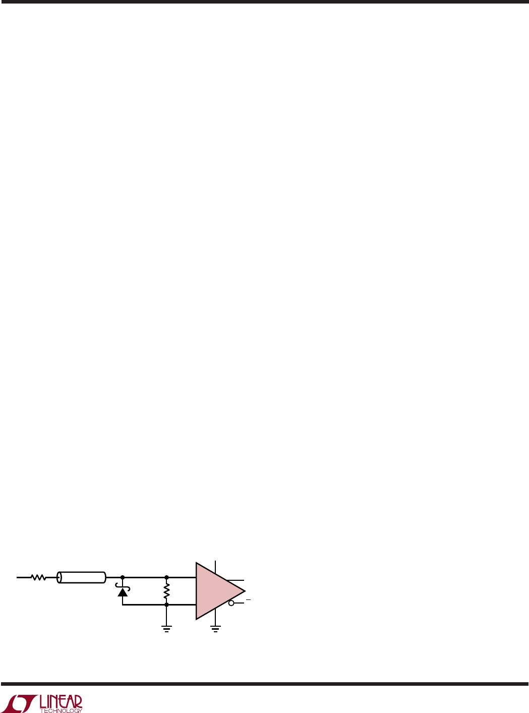
strate diode from turning on. The zero-crossing detector
in Figure 1 demonstrates the use of a fast clamp diode.
The zero-crossing detector terminates the transmission
line at its 50 characteristic impedance. Negative inputs
should not fall below –2V to keep the signal current within
the clamp diode’s maximum forward rating. Positive
inputs should not exceed the device’s absolute maximum
ratings or the power rating on the terminating resistor.
Either input may go above the positive common mode
limit without damaging the comparator. The upper voltage
limit is determined by an internal diode from each input to
the positive supply. The input may go above the positive
supply as long as it does not go far enough above it to
conduct more than 10mA. Functionality will continue if the
remaining input stays within the allowed common mode
range. There will, however, be an increase in propagation
delay as the input signal switches back into the common
mode range.
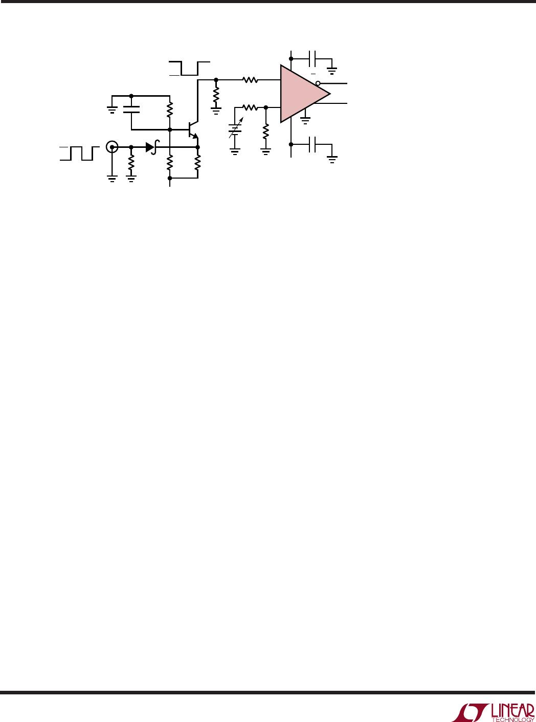
Figure 1. Fast Zero-Crossing Detector
Input Bias Current
Input bias current is measured with the output held at
1.4V. As with any PNP differential input stage, the LT1394
bias current flows out of the device. It will go to zero on an
input which is high and double on an input which is low.
LATCH Pin Dynamics
The LATCH pin is intended to retain input data (output
latched) when the LATCH pin goes high. The pin will float
to a high state when disconnected, so a flow-through
condition requires that the LATCH pin be grounded. The
LATCH pin is designed to be driven with either a TTL or
CMOS output. It has no built-in hysteresis.
To guarantee data retention, the input signal must remain
valid at least 2ns after the latch goes high (hold time), and
must be valid at least –0.4ns before the latch goes high
(setup time). The negative setup time simply means that
the data arriving 0.4ns after (rather than before) the latch
signal is valid. When the latch signal goes low, new data
will appear at the output in approximately 6ns (latch
propagation delay).
Measuring Response Time
To properly measure the response of the LT1394 requires
an input signal source with very fast rise times and
exceptionally clean settling characteristics. The last
requirement comes about because the standard compara-
tor test calls for an input step size that is large compared
to the overdrive amplitude. Typical test conditions are
100mV step size with 5mV overdrive. This requires an
input signal that settles to within 1% (1mV) of final value
in only a few nanoseconds with no ringing or settling tail.
Ordinary high speed pulse generators are not capable of
generating such a signal, and in any case, no ordinary
oscilloscope is capable of displaying the waveform to
check its fidelity. Some means must be used to inherently
generate a fast, clean edge with known final value. The
circuit shown in Figure 2 is the best electronic means of
generating a fast, clean step to test comparators. It uses
a very fast transistor in a common base configuration. The
transistor is switched off with a fast edge from the genera-
tor and the collector voltage settles to exactly 0V in just a
few nanoseconds. The most important feature of this
1394 F01
5V
+
LT1394
Q
Q
CABLE
R
T
50
V
IN
R
S
50
1N5712
8
LT1394
+
LT1394
1394 F02
FET PROBE
FET PROBE
* TOTAL LEAD LENGTH INCLUDING DEVICE PIN.
SOCKET AND CAPACITOR LEADS SHOULD BE
LESS THAN 0.5 IN. USE GROUND PLANE
** (V
OS
+ OVERDRIVE)/200
25
25
5V
0.01µF*
0.01µF
10k
50
V1**
2N3866
0V
–3V
–5V
–5V
50
PULSE
IN
750400
0.1µF
130
0V
100mV
Q
Q
APPLICATIONS INFORMATION
WUU
U
Figure 2. Response Time Test Circuit
circuit is the lack of feedthrough from the generator to the
comparator input. This prevents overshoot on the com-
parator input, which would give a false fast reading on
comparator response time.
To adjust the circuit for exactly 5mV overdrive, V1 is
adjusted so that the LT1394 output under test settles to
1.4V (in the linear region). Then V1 is changed by –1V to
set overdrive to 5mV.
High Speed Design Techniques
A substantial amount of design effort has made the LT1394
relatively easy to use. It is much less prone to oscillation
than some slower comparators, even with slow input
signals. However, as with any high speed comparator,
there are a number of pitfalls which may arise because of
PC board layout and design. The most common problems
involve power supply bypassing. Bypassing is necessary
to maintain low supply impedance. DC resistance and
inductance in supply wires and PC traces can quickly build
up to unacceptable levels. This allows the supply line to
move with changing internal current levels of the con-
nected devices. This will almost always result in improper
operation. In addition, adjacent devices connected through
an unbypassed supply can interact with each other through
the finite supply impedances. Bypass capacitors furnish a
simple solution to this problem by providing a local
reservoir of energy at the device, keeping supply imped-
ances low.
Bypass capacitors should be as close as possible to the
LT1394. A good high frequency capacitor such as a 0.1µF
ceramic is recommended, in parallel with a larger capaci-
tor such as a 4.7µF tantalum.
Poor trace routes and high source impedances are also
common sources of problems. Be sure to keep trace
lengths as short as possible, and avoid running any output
trace adjacent to an input trace to prevent unnecessary
coupling. If output traces are longer than a few inches, be
sure to terminate them with a resistor to eliminate any
reflections that may occur. Resistor values are typically
250 to 400. Also, be sure to keep source impedances
as low as possible, preferably 1k or less.
Crystal Oscillators
Figure 3’s circuits are crystal oscillators. In the circuit (a)
the resistors at the LT1394’s positive input set a DC bias
point. The 2k-0.068µF path sets up phase shifted feedback
and the circuit looks like a wideband unity-gain follower at
DC. The crystal’s path provides resonant positive feed-
back and stable oscillation occurs. The circuit (b) is
similar, but supports oscillation frequencies to 30MHz.
Above 10MHz, AT-cut crystals operate in overtone mode.
Because of this, oscillation can occur at multiples of the
desired frequency. The damper network rolls off gain at
high frequency, ensuring proper operation.
Switchable Output Crystal Oscillator
Figure 4 permits crystals to be electronically switched by
logic commands. This circuit is similar to the previous
examples, except that oscillation is only possible when
one of the logic inputs is biased high.
9
LT1394
APPLICATIONS INFORMATION
WUU
U
Temperature-Compensated Crystal Oscillator (TXCO)
Figure 5 is a temperature-compensated crystal oscillator
(TXCO). This circuit reduces oscillator temperature drift
by inserting a temperature-dependent compensatory cor-
rection into the crystal’s frequency trimming network.
This open-loop correction technique relies on cancellation
of the temperature characteristics of the oscillator, which
are quite repeatable.
The LT1394 and associated components form the crystal
oscillator, operating similarly to Figure 3’s examples. The
LM134, a temperature-dependent current source, biases
A1. A1 takes gain referred to the LM134’s output and the
negative offset supplied via the 470k-LT1004 reference
path. Note that the LT1004’s negative voltage bias is
bootstrapped from the oscillator’s output, maintaining
single supply operation. This arrangement delivers tem-
perature-dependent bias to the varactor diode, causing a
scaled variation in the crystal’s resonance versus ambient
temperature. The varactor’s bias-dependent capacitance
shift pulls crystal frequency to complement the circuit’s
temperature drift. The simple first order fit provided by the
compensation is very effective. Figure 6 shows results.
The –70ppm frequency shift over 0°C to 70°C is corrected
within a few ppm. The “FREQ SET” trim also biases the
varactor, allowing accurate output frequency setting. It is
worth noting that better compensation is possible by
including higher order terms in the temperature-to-volt-
age conversion.
18ns, 500µV Sensitivity Comparator
The ultimate limitation on comparator sensitivity is avail-
able gain. Unfortunately, increasing gain invariably
involves giving up speed. The gain vs. speed trade-off in a
fast comparator is usually a practical compromise
designed to satisfy most applications. Some situations,
however, require more sensitivity (e.g., higher gain) with
minimal impact on speed. Figure 7’s circuit adds a differ-
ential preamplifier ahead of the LT1394, increasing gain.
This permits 500µV comparisons in 18ns. A parallel path
DC stabilization approach eliminates preamplifier drift as
an error source. A1 is the differential preamplifier, operat-
ing at a gain of 100. Its output is AC-coupled to the LT1394.
Figure 3. Crystal Oscillators for Outputs to 30MHz. Circuit (b)’s
Damper Network Supresses Overtone Crystal’s Harmonic Modes
+
LT1394
2k
5V
2k
1MHz TO 10MHz
CRYSTAL (AT-CUT)
0.068µF
OUTPUT
1394 F03
2k
+
LT1394
2k
5V
2k
2k
10MHz TO 25MHz
CRYSTAL (AT-CUT)
200pF
OUTPUT
820pF
22
(a)
(b)
1394 F04
+
LT1394
1k
5V
1k
1k
75pF
D1
OUTPUT
B
A
LOGIC INPUTS
AS MANY STAGES
AS DESIRED
XTAL A
1k
R
X
XTAL B
XTAL X
D2
D
X
2k
= 1N4148
GROUND XTAL CASES
Figure 4. Switchable Output Crystal Oscillator. Biasing A or B
High Places Associated Crystal in Feedback Path. Additional
Crystal Branches Are Permissible

LT1394CS8#PBF

Mfr. #:
Manufacturer:
Analog Devices Inc.
Description:
Analog Comparators 7ns Low Power Comparator
Lifecycle:
New from this manufacturer.
Delivery:
DHL FedEx Ups TNT EMS
Payment:
T/T Paypal Visa MoneyGram Western Union