LTC3626
1
3626fa
For more information www.linear.com/LTC3626
Typical applicaTion
FeaTures DescripTion
20V, 2.5A Synchronous
Monolithic Step-Down Regulator with
Current and Temperature Monitoring
The LT C
®
3626 is a high efficiency, monolithic synchronous
buck regulator using a phase-lockable controlled on-time,
current mode architecture capable of supplying up to 2.5A
of output current. The operating supply voltage range is
3.6V to 20V, making it suitable for a wide range of power
supply applications.
The operating frequency is programmable from 500kHz to
3MHz with an external resistor allowing the use of small
surface mount inductors. For applications sensitive to
switching noise, the LTC3626 can be externally synchro
-
nized over the same frequency range. An internal phase-
locked loop aligns the on-time of the top power MOSFET to
the in
ternal or external clock. This unique controlled on-time
architecture is ideal for high step-down ratio applications
that demand high switching frequencies and fast transient
response. An internal phase lock loop servos the on-time
of the internal one-shot timer to match the frequency of
the internal clock or an applied external clock.
The LTC3626 offers two operational modes: Burst
Mode and forced continuous mode to allow the user
to optimize output voltage ripple, noise and light load
efficiency for a given application.
applicaTions
n
3.6V to 20V Input Voltage Range
n
Wide Output Voltage Range of 0.6V to 97% V
IN
Opti-
mized for 0.6V to 6V
n
Low R
DS(ON)
Integrated Switches Provide Up to 95%
Efficiency
n
Up to 2.5A of Output Current
n
Average Input and Output Current Monitoring
n
Programmable Average Input/Output Current Limit
n
Die Temperature Monitor and Programmable Limit
n
Adjustable Switching Frequency: 500kHz to 3MHz
n
External Frequency Synchronization
n
Current Mode Operation for Excellent Line and Load
Transient Response
n
0.6V Reference with 1% Accuracy Over Temperature
n
User Selectable Burst Mode
®
Operation or Forced
Continuous Operation
n
Short-Circuit Protected
n
Output Voltage Tracking Capability
n
Power Good Status Output
n
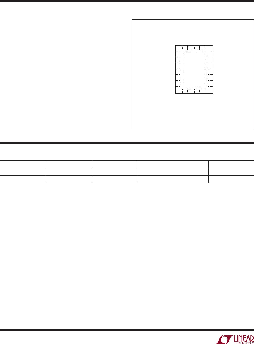
Available in Small, Thermally Enhanced, 20-Lead
(3mm × 4mm) QFN Package
n
Distributed Power Systems
n
Battery-Powered Instruments
n
Point-of-Load Power Supply
L, LT , LT C , LT M , Burst Mode, Linear Technology and the Linear logo are registered and Hot
Swap is a trademark of Linear Technology Corporation. All other trademarks are the property
of their respective owners. Protected by U.S. Patents, including 5481178, 5847554, 6580258,
6304066, 6476589, 6774611, 5994885.
PV
IN
SV
IN
RUN
BOOST
SW
V
ON
FB
PGOOD
INTV
CC
TRACK/SS
ITH
MODE/SYNC
TSET
IMON
IN
TMON
IMON
OUT
SGND PGND
LTC3626
47µF
47µF
V
OUT
3.3V
2.5A
V
IN
3.6V TO 20V
5.1k
F
2.2µF
0.1µF
22pF
2.2µH
115k
25.5k
3626 TA01
324k
RT
Efficiency vs Load Current
LOAD CURRENT (mA)
30
EFFICIENCY (%)
POWER LOSS (W)
90
100
20
10
80
50
70
60
40
1 100 1000 10000
3626 TA01b
0
0.01
10
1
0.1
0.001
10
Burst Mode
OPERATION
V
IN
= 12V
V
IN
= 5V
V
OUT
= 3.3V
LTC3626
2
3626fa
For more information www.linear.com/LTC3626
absoluTe MaxiMuM raTings
PV
IN
........................................................... 0.3V to 22V
SV
IN
........................................................... 0.3V to 22V
BOOST .................................................... 0.3V to 25.6V
BOOST-SW ................................................ 0.3V to 3.6V
INTV
CC
...................................................... 0.3V to 3.6V
ITH, RT, FB ................................. 0.3V to INTV
CC
+ 0.3V
MODE/SYNC ..............................0.3V to INTV
CC
+ 0.3V
TRACK/SS, IMON
IN
, IMON
OUT
...0.3V to INTV
CC
+ 0.3V
TSET, TMON ..............................0.3V to INTV
CC
+ 0.3V
SW, RUN .......................................... 0.3V to V
IN
+ 0.3V
PGOOD ....................................................... 0.3V to 22V
V
ON
............................................................ 0.3V to 18V
SW Source Current (DC, Note 2) ..............................2.5A
Operating Junction Temperature Range
(Notes 3, 4) ........................................... 40°C to 125°C
Storage Temperature Range .................. 6C to 150°C
(Note 1)
20 19 18 17
7 8
TOP VIEW
21
PGND
UDC PACKAGE
20-LEAD (3mm × 4mm) PLASTIC QFN
9 10
6
5
4
3
2
1
11
12
13
14
15
16
BOOST
INTV
CC
V
ON
TSET
TMON
SGND
PV
IN
PV
IN
SV
IN
RUN
RT
ITH
SW
SW
PGOOD
MODE/SYNC
IMON
IN
IMON
OUT
TRACK/SS
FB
T
JMAX
= 125°C, θ
JA
= 47°C/W
EXPOSED PAD (PIN 21) IS PGND, MUST BE SOLDERED TO PCB
pin conFiguraTion
orDer inForMaTion
LEAD FREE FINISH TAPE AND REEL PART MARKING* PACKAGE DESCRIPTION TEMPERATURE RANGE
LTC3626EUDC#PBF LTC3626EUDC#TRPBF LGCC 20-Lead (3mm × 4mm) Plastic QFN –40°C to 125°C
LTC3626IUDC#PBF LTC3626IUDC#TRPBF LGCC 20-Lead (3mm × 4mm) Plastic QFN –40°C to 125°C
Consult LTC Marketing for parts specified with wider operating temperature ranges. *The temperature grade is identified by a label on the shipping container.
Consult LTC Marketing for information on non-standard lead based finish parts.
For more information on lead free part marking, go to:
http://www.linear.com/leadfree/
For more information on tape and reel specifications, go to: http://www.linear.com/tapeandreel/
LTC3626
3
3626fa
For more information www.linear.com/LTC3626
elecTrical characTerisTics
The l denotes the specifications which apply over the specified operating
junction temperature range, otherwise specifications are at T
A
= 25°C (Note 3). PV
IN
= SV
IN
=
12V unless otherwise specified.
SYMBOL PARAMETER CONDITIONS MIN TYP MAX UNITS
PV
IN
Input Supply Range
l
3.0 20 V
SV
IN
Input Supply Range
l
3.6 20 V
V
VOUT
Output Voltage Range (Note 5) V
ON
= V
OUT
0.6 6 V
I
Q
Input DC Supply Current
Forced Continuous Operation
PV
IN
SV
IN
MODE = 0, R
RT
= 158k, IMON
IN
, IMON
OUT
,
TMON, TSET = INTV
CC
30
900
39
1200
µA
µA
Sleep Current
PV
IN
SV
IN
V
FB
> 0.6V, IMON
IN
, IMON
OUT
, TMON, TSET,
MODE = INTV
CC
30
270
39
350
µA
µA
Shutdown
PV
IN
SV
IN
I
LOAD
= 0A, V
RUN
= 0V
0.01
13
2
17
µA
µA
V
FB
Feedback Reference Voltage
l
0.594 0.600 0.606 V
V
LINE(REG)
V
FB
Line Regulation PV
IN
= SV
VIN
= 3.6V to 20V 0.01 %/V
V
LOAD(REG)
V
FB
Load Regulation ITH = 0.6V to 1.5V 0.1 %
Feedback Pin Input Current V
FB
= 0.6V ±30 nA
Error Amplifier Transconductance ITH = 1.2V 1.5 mS
t
ON(MIN)
Minimum On-Time V
VON
=1V, PV
IN
= SV
VIN
= 3.6V 20 ns
t
OFF(MIN)
Minimum Off-Time PV
IN
= SV
IN
= 6V 40 60 ns
Valley Switch Current Limit 2.4 2.9 3.6 A
Negative Valley Switch Current Limit –1 A
f
OSC
Oscillator Frequency V
RT
= INTV
CC
R
RT
= 158k
R
RT
= 105k
1.4
1.7
2.5
2
2
3
2.6
2.3
3.5
MHz
MHz
MHz
R
DS(ON)
Top Switch On-Resistance
Bottom Switch On-Resistance
115
70
IMON
OUT
Current (Note 6) I
SW
= 2.5A
I
SW
= 1.5A
I
SW
= 0.5A
148.5
89.1
29.7
156.25
93.75
31.25
164.0
98.4
33.5
µA
µA
µA
I
OUT
Limit Regulation Voltage
l
1.15 1.22 1.28 V
IMON
IN
Current (Note 6) I
SW
= 2.5A, 20% Duty Cycle
I
SW
= 1.5A, 20% Duty Cycle
I
SW
= 0.5A, 20% Duty Cycle
29.7
17.8
5.9
31.25
18.75
6.25
32.8
19.7
6.7
µA
µA
µA
I
IN
Limit Regulation Voltage
l
1.15 1.22 1.28 V
Internal Temperature Monitor T
A
= 25°C 1.5 V
Internal Temperature Monitor Slope (Note 7) 200 °C/V
Temperature Limit Hysteresis 50 mV
PV
IN
Overvoltage Lockout Threshold PV
IN
Rising
PV
IN
Falling
20
21.5
20.5
V
V
V
INTVCC
INTV
CC
Voltage 3.6V < PV
IN
= SV
VIN
< 20V 3.1 3.3 3.5 V
INTV
CC
Load Regulation (Note 8) I
INTVCC
= 0mA to 20mA 0.6 %
V
RUN
RUN Threshold RUN Rising
RUN Falling
l
l
1.19
0.97
1.23
1.0
1.27
1.03
V
V
RUN Leakage Current PV
VIN
= SV
VIN
= 20V 0 ±1 μA

LTC3626IUDC#PBF

Mfr. #:
Manufacturer:
Analog Devices / Linear Technology
Description:
Switching Voltage Regulators 3A, 20V Monolithic Step-Down Regulator with Current and Temperature Monitoring
Lifecycle:
New from this manufacturer.
Delivery:
DHL FedEx Ups TNT EMS
Payment:
T/T Paypal Visa MoneyGram Western Union