LTC3626
16
3626fa
For more information www.linear.com/LTC3626
applicaTions inForMaTion
results. Furthermore, this supply is intended only to supply
additional DC load currents as desired and not intended to
regulate large transient or AC behavior as this may impact
LTC3626 operation.
Boost Capacitor
The boost capacitor, C
BST
, on the Functional Diagram
is used to create a voltage rail above the applied input
voltage, V
IN
. Specifically, the boost capacitor is charged
to a voltage equal to approximately INTV
CC
each time the
bottom power MOSFET is turned on. The charge on this
capacitor is then used to supply the required transient
current during the remainder of the switching cycle. When
the top MOSFET is turned on, the BOOST pin voltage will
be equal to approximately V
IN
+ 3.3V. For most applica-
tions a 0.1μF ceramic capacitor will provide adequate
performance.
Output V
oltage Programming
The LTC3626 will adjust the output voltage such that V
FB
equals the reference voltage of 0.6V according to:
V
OUT
= 0.6V 1+
R1
R2
The desired output voltage is set by the appropriate selec-
tion of resistors R1 and R2 as shown in Figure 2. Choosing
large values for R1 and R
2 will result in improved efficiency
but may lead to undesired noise coupling or phase margin
reduction due to stray capacitance at the FB node. Care
should be taken to route the FB line away from any noise
source, such as the SW or BOOST lines.
To improve the frequency response of the main control
loop a feedforward capacitor, C
F
, may be used as shown
in Figure 2.
Minimum Off-Time/On-Time Considerations
The minimum off-time is the smallest amount of time that
the LTC3626 requires to turn on the bottom power MOS
-
FET, trip the current comparator and turn off the power
MOSFET.
This time is typically 40ns. For the controlled
on-time current mode control architecture, the minimum
off-time limit imposes a maximum duty cycle of:
DC
MAX
= 1 – (f t
OFF(MIN)
)
where f is the switching frequency and t
OFF(MIN)
is the
minimum off-time. If the maximum duty cycle is surpassed,
due to a dropping input voltage for example, the output
will drop out of regulation. The minimum input voltage to
avoid this dropout condition is:
V
IN(MIN)
=
V
OUT
1 f t
OFF(MIN)
( )
Users should consider reducing the LTC3626 operating
frequency for applications that may violate the minimum
off-time if constant regulation is required.
Conversely, the minimum on-time is the smallest dura
-
tion of time in which the top power MOSFET can be in
its “on”
state. This time is typically 20ns. In continuous
mode operation, the minimum on-time limit imposes a
minimum duty cycle of:
DC
MIN
= (f t
ON(MIN)
)
where t
ON(MIN)
is the minimum on-time. As the equation
shows, reducing the operating frequency will alleviate the
minimum duty cycle constraint.
In rare cases in which the LTC3626’s minimum duty
cycle is surpassed, the output voltage will still remain in
regulation, however the switching frequency will be lower
than its programmed value. This is an acceptable result in
many applications, so high switching frequencies may be
used in the design without fear of severe consequences.
As the sections on Inductor and Capacitor Selection show,
high switching frequencies allow the use of smaller board
components, thus reducing the footprint of the applica
-
tion circuit.
FB
R1
R2
C
F
3626 F02
V
OUT
SGND
LTC3626
Figure 2. Optional Feedforward Capacitor
LTC3626
17
3626fa
For more information www.linear.com/LTC3626
applicaTions inForMaTion
Internal/External Loop Compensation
The LTC3626 provides the option to use a fixed internal
loop compensation network to reduce both the required
external component count and design time. The internal
loop compensation network can be selected by connect
-
ing the ITH pin to the INTV
CC
pin. To ensure stability, it
is recommended that the internal compensation be used
at operating frequencies of 1MHz or greater. When using
internal compensation, a reasonable starting point for
the minimum amount of output capacitance necessary
for stability can be found as the greater of either 22µF or
C
OUT
defined by the equation:
C
OUT
>
70e-6
V
OUT
Alternatively, the user may choose specific external loop
compensation components to optimize the main control
loop transient response as desired. External loop com
-
pensation is chosen by simply connecting the desired
network to the ITH pin.
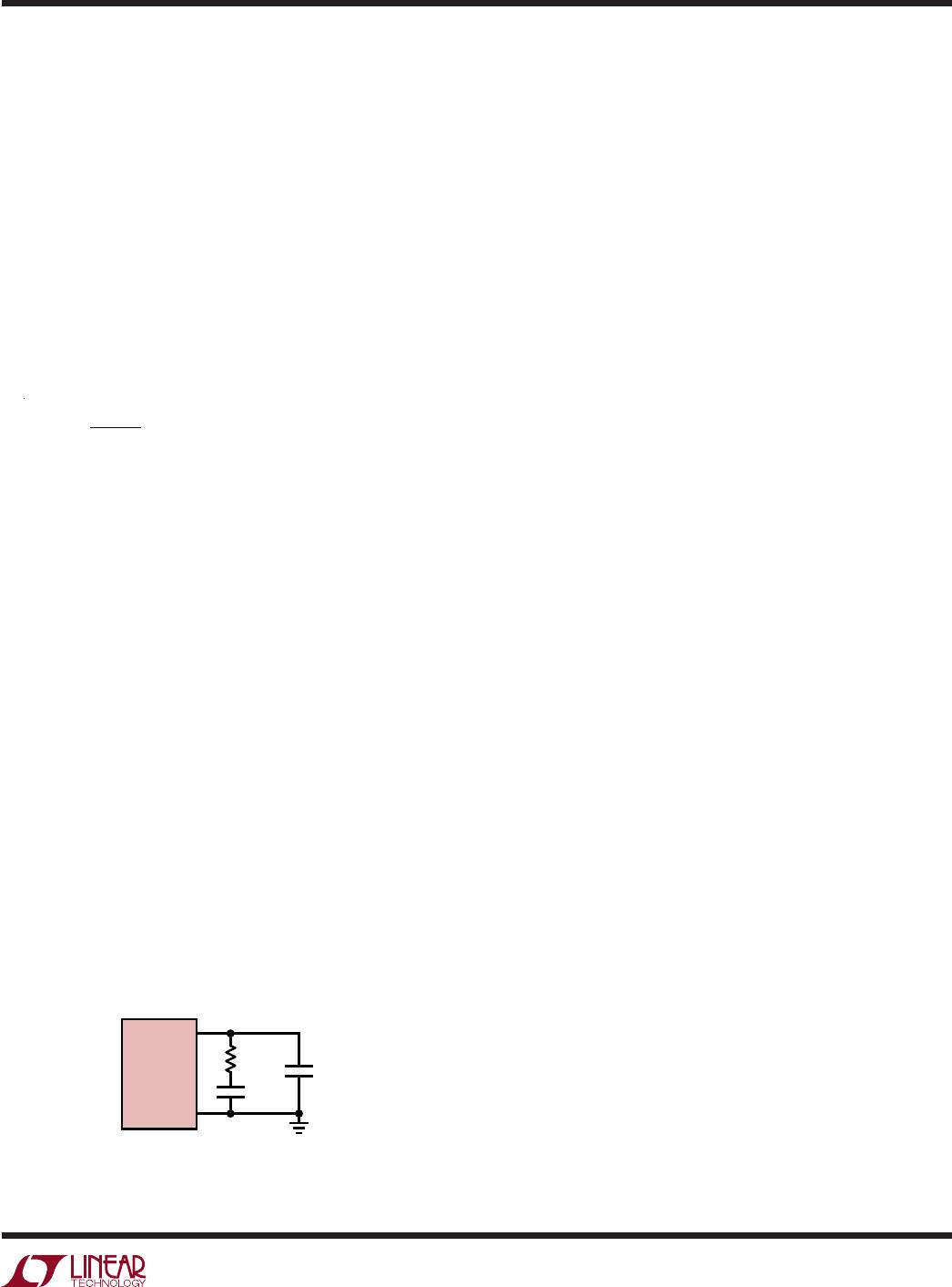
Suggested compensation component values are shown
in Figure 3. For a 2MHz application, an R-C (R
COMP
and
C
COMP
in Figure 3) network of 220pF and 13kΩ provides
a good starting point. The bandwidth of the loop increases
with decreasing C. If R is increased by the same factor
that C is decreased, the zero frequency will be kept the
same, thereby keeping the phase the same in the most
critical frequency range of the feedback loop. A 10pF
bypass capacitor (C
BYP
in Figure 3) the ITH pin is recom-
mended to filter out high frequency coupling from stray
board capacitance.
In addition, a feedforward capacitor,
C
F
, can be added to improve the high frequency response,
as previously shown in Figure 2. Capacitor C
F
provides
phase lead by creating a high frequency zero with R1
which improves the phase margin.
Checking Transient Response
The regulator loop response can be checked by observing
the response of the system to a load step. When configured
for external compensation, the availability of the ITH pin
not only allows optimization of the control loop behavior
but also provides a DC-coupled and AC-filtered closed-loop
response test point. The DC step, rise time, and settling
behavior at this test point reflect the systems closed-
loop response. Assuming a predominantly second order
system, the phase margin and/or damping factor can be
estimated by observing the percentage of overshoot seen
at this pin with a high impedance, low capacitance probe.
The ITH external components shown in Figure 3 will pro
-
vide an adequate starting point for most applications. The
series R-C filter sets the pole-zero loop compensation. The
values can be modified slightly, from approximately 0.5
to 2 times their suggested values, to optimize transient
response once the final PC layout is done and the particular
output capacitor type and value have been determined.
The specific output capacitors must be selected because
their various types and values determine the loop feedback
factor, gain, and phase. An output current pulse of 20%
to 100% of full load current, with a rise time of s to
10μs, will produce output voltage and ITH pin waveforms
that will give a sense of the overall loop stability without
breaking the feedback loop.
When observing the response of V
OUT
to a load step, the
initial output voltage step may not be within the bandwidth
of the feedback loop. As a result, the standard second
order overshoot/DC ratio cannot be used to estimate
phase margin. The output voltage settling behavior is
related to the stability of the closed-loop system and will
demonstrate the actual overall supply performance. For
a detailed explanation of optimizing the compensation
components, including a review of control loop theory,
refer to Linear Technology Application Note 76. As shown
in Figure 2 a feed-forward capacitor, C
F
, may be added
across feedback resistor R1 to improve the high frequency
response of the system. Capacitor C
F
provides phase lead
by creating a high frequency zero with R1.
ITH
R
COMP
13k
C
COMP
220pF
C
BYP
3626 F03
SGND
LTC3626
Figure 3. Compensation Components
LTC3626
18
3626fa
For more information www.linear.com/LTC3626
applicaTions inForMaTion
In some applications severe transients can be caused by
switching in loads with large (>10μF) input capacitors. The
discharged input capacitors are effectively put in parallel
with C
OUT
, causing a rapid drop in V
OUT
. No regulator can
deliver enough current to prevent this output droop if the
switch connecting the load has low resistance and is driven
quickly. The solution is to limit the turn-on speed of the
load switch driver. A Hot Swap controller is designed
specifically for this purpose and usually incorporates cur
-
rent limit, short-circuit protection and soft-start functions.
Input/Output Current Monitor and Limit
The LTC3626 senses the average current through the
synchronous switch during the on state and outputs a
scaled replica of this current (which corresponds to the
regulator’s load current) to the IMON
OUT
pin. A mirrored
version of this signal is modulated with the buck regula-
tor’s duty cycle to provide a scaled replica of the buck
regulator
s input current to the IMON
IN
pin. The average
current at each of the monitor pins is 1/16000th the
measured average current. The output current at either
pin may be measured directly or converted to a voltage
with an external resistor.
The average input and output current monitor circuits
both use a chopping technique to achieve high accuracy.
As a result, a small periodic ripple may be seen at either
of these outputs, the average of which is the measured
value of interest. The ripple frequency will be the operating
frequency divided by 256. In addition, the average input
current is measured by modulating the duty cycle of the
average output current leading to an additional ripple at
the operating frequency. If required, a capacitor may be
placed on either output pin to reduce the magnitude of
the ripple.
The voltages at the IMON
OUT
and IMON
IN
pins are con-
tinuously fed to independent current limit amplifiers that
have a voltage reference of 1.2V (typical).
A programmable
average current limit for either average output current or
average input current may be obtained by placing a resis
-
tor, R
LIM
, from the monitor pin to SGND according to the
following equation:
R
LIM
=
1.2V 16000
I
LIM
where I
LIM
is the programmed current limit.
When active, the current limit amplifiers form a feedback
loop that controls the maximum average current produced
by the LTC3626. Thus, when using the current limit fea
-
ture, a compensation capacitor should be placed between
SGND and the monitor pin of interest.
This capacitor,
combined with the R
LIM
resistor, is intended to create a
dominant pole for compensation purposes. For most ap-
plications, a capacitor with a minimum value of F will
provide adequate loop stability
.
However, given the wide
variation in loop parameters that depend on specific ap
-
plication requirements, loop stability should be confirmed
by stepping the load current to a level that triggers the
programmed current limit. The resultant transient response
should provide a sense of the overall loop stability with
-
out breaking the feedback loop. The transient response
that results from releasing the current limit should also
be checked.
If the transient response waveforms exhibit
excessive ringing, indicating inadequate loop stability,
increase the compensation capacitor value until adequate
stability has been achieved.
The simple dominant pole compensation scheme dis
-
cussed previously is intended to provide loop stability by
limiting the bandwidth of the current limit feedback loop.
As a result
, the average current may momentarily exceed
the programmed limit until the current limit feedback loop
can respond. More advanced compensation networks may
be used to potentially reduce the loop response time but
generally require more caution and design expertise. For
example, one technique is to add a low value resistor in

LTC3626IUDC#PBF

Mfr. #:
Manufacturer:
Analog Devices / Linear Technology
Description:
Switching Voltage Regulators 3A, 20V Monolithic Step-Down Regulator with Current and Temperature Monitoring
Lifecycle:
New from this manufacturer.
Delivery:
DHL FedEx Ups TNT EMS
Payment:
T/T Paypal Visa MoneyGram Western Union