2-OUTPUT 1.8V PCIE GEN1/2/3 ZERO DELAY / FANOUT BUFFER 10 REVISION F 04/28/16
9DBV0231 DATASHEET
General SMBus Serial Interface Information
How to Write
Controller (host) sends a start bit
Controller (host) sends the write address
IDT clock will acknowledge
Controller (host) sends the beginning byte location = N
IDT clock will acknowledge
Controller (host) sends the byte count = X
IDT clock will acknowledge
Controller (host) starts sending Byte N through Byte
N+X-1
IDT clock will acknowledge each byte one at a time
Controller (host) sends a Stop bit
Note: SMBus Address is 1101101x, where x is the
read/write bit.
How to Read
Controller (host) will send a start bit
Controller (host) sends the write address
IDT clock will acknowledge
Controller (host) sends the beginning byte location = N
IDT clock will acknowledge
Controller (host) will send a separate start bit
Controller (host) sends the read address
IDT clock will acknowledge
IDT clock will send the data byte count = X
IDT clock sends Byte N+X-1
IDT clock sends Byte 0 through Byte X (if X
(H)
was
written to Byte 8)
Controller (host) will need to acknowledge each byte
Controller (host) will send a not acknowledge bit
Controller (host) will send a stop bit
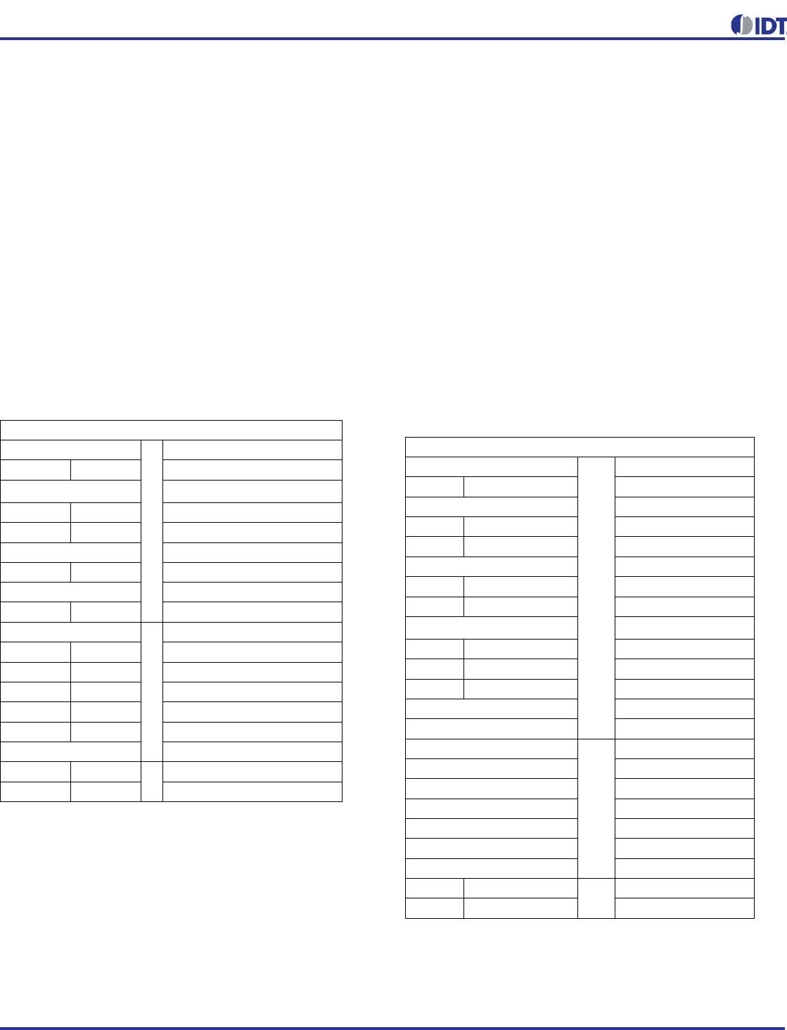
Index Block Write Operation
Controller (Host) IDT (Slave/Receiver)
TstarT bit
Slave Address
WR WRite
ACK
Beginning Byte = N
ACK
Data Byte Count = X
ACK
Beginning Byte N
X Byte
ACK
O
OO
OO
O
Byte N + X - 1
ACK
PstoP bit
Index Block Read Operation
Controller (Host) IDT (Slave/Receiver)
TstarT bit
Slave Address
WR WRite
ACK
Beginning Byte = N
ACK
RT Repeat starT
Slave Address
RD ReaD
ACK
Data Byte Count=X
ACK
X Byte
Beginning Byte N
ACK
O
OO
OO
O
Byte N + X - 1
N Not acknowledge
PstoP bit
REVISION F 04/28/16 11 2-OUTPUT 1.8V PCIE GEN1/2/3 ZERO DELAY / FANOUT BUFFER
9DBV0231 DATASHEET
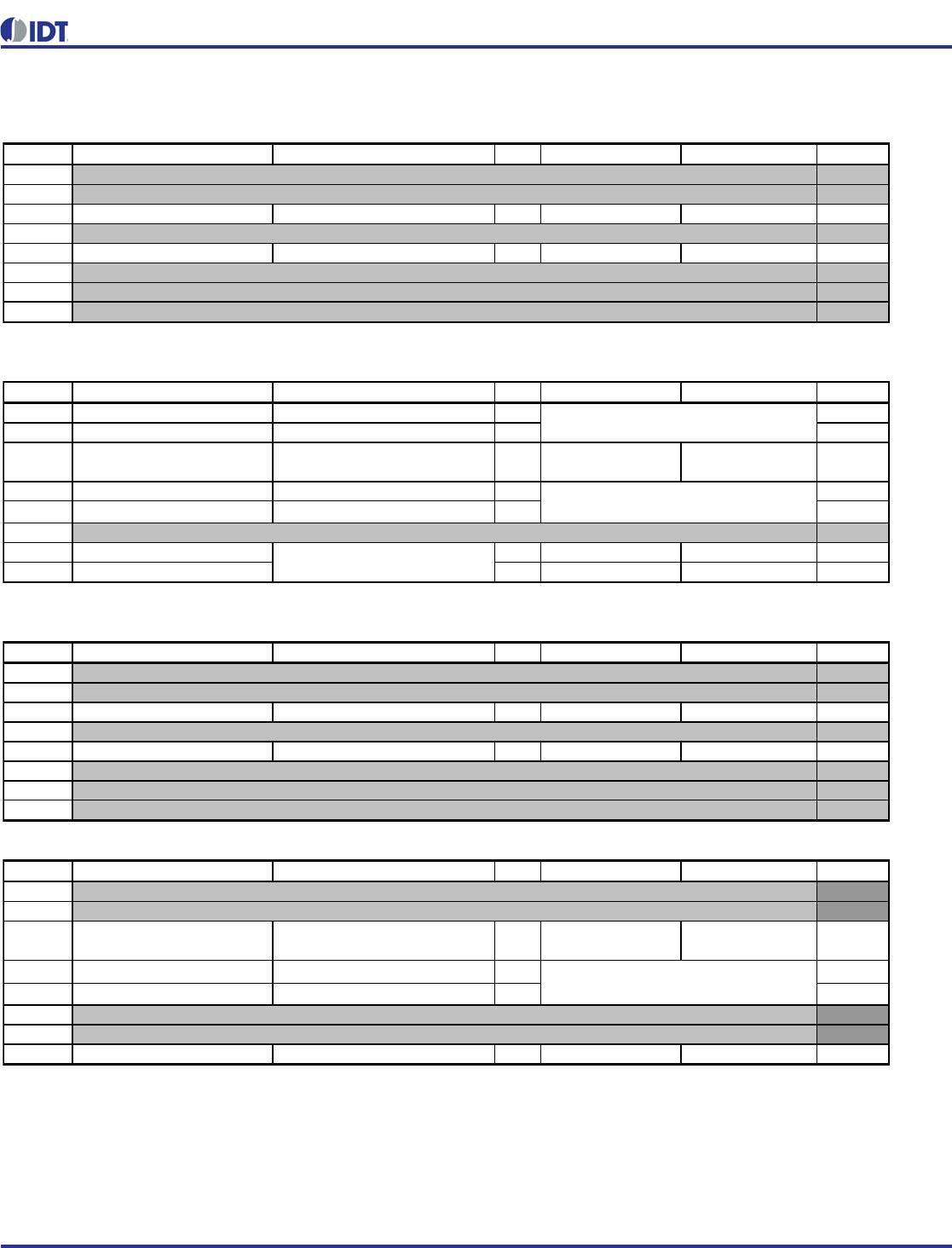
SMBus Table: Output Enable Register
1
Byte 0 Name Control Function Type 0 1 Default
Bit 7
1
Bit 6
1
Bit 5
DIF OE1 Output Enable RW Low/Low Enabled 1
Bit 4
1
Bit 3
DIF OE0 Output Enable RW Low/Low Enabled 1
Bit 2
1
Bit 1
1
Bit 0
1
1. A low on these bits will overide the OE# pin and force the differential output Low/Low
SMBus Table: PLL Operating Mode and Output Amplitude Control Register
Byte 1 Name Control Function Type 0 1 Default
Bit 7
PLLMODERB1 PLL Mode Readback Bit 1
R
Latch
Bit 6
PLLMODERB0 PLL Mode Readback Bit 0
R
Latch
Bit 5
PLLMODE_SWCNTRL Enable SW control of PLL Mode RW
Values in B1[7:6]
set PLL Mode
Values in B1[4:3]
set PLL Mode
0
Bit 4
PLLMODE1 PLL Mode Control Bit 1
RW
1
0
Bit 3
PLLMODE0 PLL Mode Control Bit 0
RW
1
0
Bit 2
1
Bit 1
AMPLITUDE 1 RW 00 = 0.6V 01 = 0.7V 1
Bit 0
AMPLITUDE 0 RW 10= 0.8V 11 = 0.9V 0
1. B1[5] must be set to a 1 for these bits to have any effect on the part.
SMBus Table: DIF Slew Rate Control Register
Byte 2 Name Control Function Type 0 1 Default
Bit 7
1
Bit 6
1
Bit 5
SLEWRATESEL DIF1 Slew Rate Selection RW Slow setting Fast setting 1
Bit 4
1
Bit 3
SLEWRATESEL DIF0 Slew Rate Selection RW Slow setting Fast setting 1
Bit 2
1
Bit 1
1
Bit 0
1
SMBus Table: Frequency Select Control Register
Byte 3 Name Control Function Type 0 1 Default
Bit 7
1
Bit 6
1
Bit 5
FREQ_SEL_EN
Enable SW selection of
frequency
RW
SW frequency
change disabled
SW frequency
change enabled
0
Bit 4
FSEL1 Freq. Select Bit 1
RW
1
0
Bit 3
FSEL0 Freq. Select Bit 0
RW
1
0
Bit 2
1
Bit 1
1
Bit 0
SLEWRATESEL FB Adjust Slew Rate of FB RW Slow setting Fast setting 1
1. B3[5] must be set to a 1 for these bits to have any effect on the part.
Byte 4 is Reserved and reads back 'hFF
Controls Output Amplitude
Reserved
Reserved
See PLL Operating Mode Table
Reserved
Reserved
Reserved
See Frequency Select Table
Reserved
Reserved
Reserved
Reserved
Reserved
See PLL Operating Mode Table
Reserved
Reserved
Reserved
Reserved
Reserved
Reserved
Reserved
2-OUTPUT 1.8V PCIE GEN1/2/3 ZERO DELAY / FANOUT BUFFER 12 REVISION F 04/28/16
9DBV0231 DATASHEET
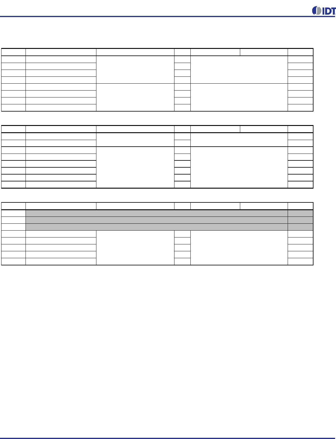
SMBus Table: Revision and Vendor ID Register
Byte 5 Name Control Function Type 0 1 Default
Bit 7
RID3
R
0
Bit 6
RID2
R
0
Bit 5
RID1
R
0
Bit 4
RID0
R
0
Bit 3
VID3
R
0
Bit 2
VID2
R
0
Bit 1
VID1
R
0
Bit 0
VID0
R
1
SMBus Table: Device Type/Device ID
Byte 6 Name Control Function Type 0 1 Default
Bit 7
Device Type1
R
0
Bit 6
Device Type0
R
1
Bit 5
Device ID5
R
0
Bit 4
Device ID4
R
0
Bit 3
Device ID3
R
0
Bit 2
Device ID2
R
0
Bit 1
Device ID1
R
1
Bit 0
Device ID0
R
0
SMBus Table: Byte Count Register
Byte 7 Name Control Function Type 0 1 Default
Bit 7
0
Bit 6
0
Bit 5
0
Bit 4
BC4 RW 0
Bit 3
BC3 RW 1
Bit 2
BC2 RW 0
Bit 1
BC1 RW 0
Bit 0
BC0 RW 0
A rev = 0000Revision ID
0001 = IDT
Device Type
Writing to this register will configure how
many bytes will be read back, default is
= 8 bytes.
VENDOR ID
000100 binary or 02 hex
00 = FGx, 01 = DBx,
10 = DMx, 11= Reserved
Device ID
Reserved
Reserved
Byte Count Programming
Reserved

9DBV0231AKILFT

Mfr. #:
Manufacturer:
IDT
Description:
Clock Buffer 2 O/P 1.8V PCIE BUFFER
Lifecycle:
New from this manufacturer.
Delivery:
DHL FedEx Ups TNT EMS
Payment:
T/T Paypal Visa MoneyGram Western Union

Products related to this Datasheet