Expand menu
Hello, Sign in
My Account
0
Cart
Home
Products
Sensors
Semiconductors
Passive Components
Connectors
Power
Electromechanical
Optoelectronics
Circuit Protection
Integrated Circuits - ICs
Main Products
Manufacturers
Blog
Services
About OMO
About Us
Contact Us
Check Stock
9DBV0231AKILFT
P1-P3
P4-P6
P7-P9
P10-P12
P13-P15
P16-P17
REVISION F 04/28/16
13
2-OUTPUT 1.8V PC
IE GEN1/2/3 ZERO DELAY / FANOUT BUFFE
R
9DBV0231 DATASHEET
Marking Diagrams
Notes:
1. “LOT” is
the lot sequ
ence numbe
r
.
2. YYWW is the last two digits of the
ye
ar and week that the part was assembled.
3. Line 2: truncated pa
rt number
4. “L” denotes RoHS compliant package.
5. “I” denotes ind
ustrial temp
erature rang
e device.
Thermal Characteristics
LOT
031AIL
YYWW
LOT
031AL
YYWW
PAR
AMET
ER
SYMBO
L
C
ON
D
ITIO
N
S
PKG
TYP
VAL
U
E
UNI
T
S
NOT
E
S
θ
JC
Ju
n
c
tio
n
to
C
a
se
6
2
°
C/
W
1
θ
Jb
Ju
n
c
tio
n
to
Ba
se
5
.4
°
C/
W
1
θ
JA
0
Ju
n
c
tio
n
to
Air
, still
ai
r
5
0
°
C/
W
1
θ
JA
1
Ju
n
c
tio
n
to Ai
r
, 1
m/s a
ir
flo
w
4
3
°
C/
W
1
θ
JA
3
Ju
n
c
tio
n
to Ai
r
, 3
m/s a
ir
flo
w
3
9
°
C/
W
1
θ
JA
5
Ju
n
c
tio
n
to Ai
r
, 5
m/s a
ir
flo
w
3
8
°
C/
W
1
1
eP
ad s
oldered t
o board
NLG
2
0
NLG
2
4
T
h
e
r
ma
l R
e
sist
a
n
ce
2-OUTPUT 1.8V PCIE GEN1/2/3 ZERO DELAY / FANOUT BUFFER
14
REVISION F 04/28/16
9DBV0231 DATASHEET
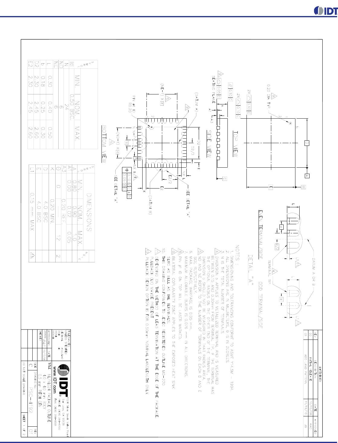
Package Outline and Dimensions
(NLG24)
REVISION F 04/28/16
15
2-OUTPUT 1.8V PC
IE GEN1/2/3 ZERO DELAY / FANOUT BUFFE
R
9DBV0231 DATASHEET
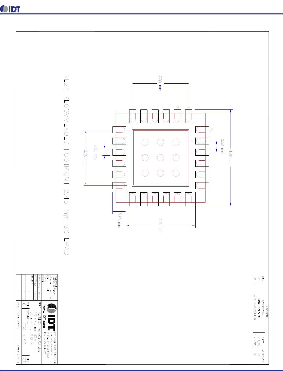
Package Outline and Dimensions
(NLG24), cont.
P1-P3
P4-P6
P7-P9
P10-P12
P13-P15
P16-P17
9DBV0231AKILFT
Mfr. #:
Buy 9DBV0231AKILFT
Manufacturer:
IDT
Description:
Clock Buffer 2 O/P 1.8V PCIE BUFFER
Lifecycle:
New from this manufacturer.
Delivery:
DHL
FedEx
Ups
TNT
EMS
Payment:
T/T
Paypal
Visa
MoneyGram
Western
Union
Products related to this Datasheet
9DBV0231AKLFT
9DBV0231AKILF
9DBV0231AKLF
9DBV0231AKILFT