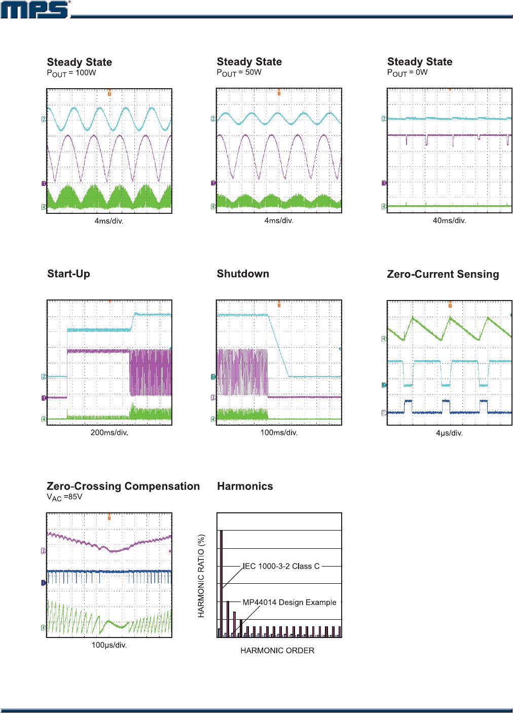
MP44014 – BOUNDARY MODE PFC CONTROLLER
MP44014 Rev. 1.01 www.MonolithicPower.com 8
11/10/2015 MPS Proprietary Information. Patent Protected. Unauthorized Photocopy and Duplication Prohibited.
© 2015 MPS. All Rights Reserved.
PIN FUNCTIONS
Pin # Name Description
1 FB Feedback. The output voltage is fed into FB through a resistor divider.
2 COMP
Output of the error amplifier. A compensation network is connected between COMP and
FB.
3 MULT
Input of the multiplier. Connect MULT to the rectified main voltage via a resistor divider to
provide the sinusoidal reference for the current control loop.
4 CS
Current sense. The current through the MOSFET is fed into CS via a resistor. The resulting
voltage on CS is compared with the output of the internal multiplier to get an internal
sinusoidal-shaped reference to determine the MOSFET’s turn-off. The on-chip R/C filter can
reduce high frequency noise on CS. Also, suggest to add a RC filter on the CS pin in case of
switching noise is too large.
5 ZCS
Inductor’s zero-crossing current sensing input. A negative transition edge triggers the
MOSFET’s turn-on. Suggest to connect a 22pF cap from this ZCS to GND to tune ZVS point.
6 GND
Ground.
7 GATE
Gate driver output. The high output current of the gate driver is able to drive a low-cost
power MOSFET. The high-level voltage of GATE is clamped to 12V in case GATE is supplied
with a high VCC.
8 VCC
Supply voltage for both the signal path of the IC and the gate driver. A bypass capacitor
from VCC to ground is needed to reduce noise.