General Description
The MAX7033 fully integrated low-power CMOS super-
heterodyne receiver is ideal for receiving amplitude-
shift-keyed (ASK) data in the 300MHz to 450MHz
frequency range. The receiver has an RF input signal
range of -114dBm to 0dBm. With few external compo-
nents and a low-current power-down mode, it is ideal
for cost-sensitive and power-sensitive applications typi-
cal in the automotive and consumer markets. The
MAX7033 consists of a low-noise amplifier (LNA), a fully
differential image-rejection mixer, an on-chip phase-
locked loop (PLL) with integrated voltage-controlled
oscillator (VCO), a 10.7MHz IF limiting amplifier stage
with received-signal-strength indicator (RSSI), and ana-
log baseband data-recovery circuitry. The MAX7033
also has a discrete one-step automatic gain control
(AGC) that reduces the LNA gain by 35dB when the RF
input signal exceeds -62dBm. The AGC circuitry offers
an externally controlled hold feature.
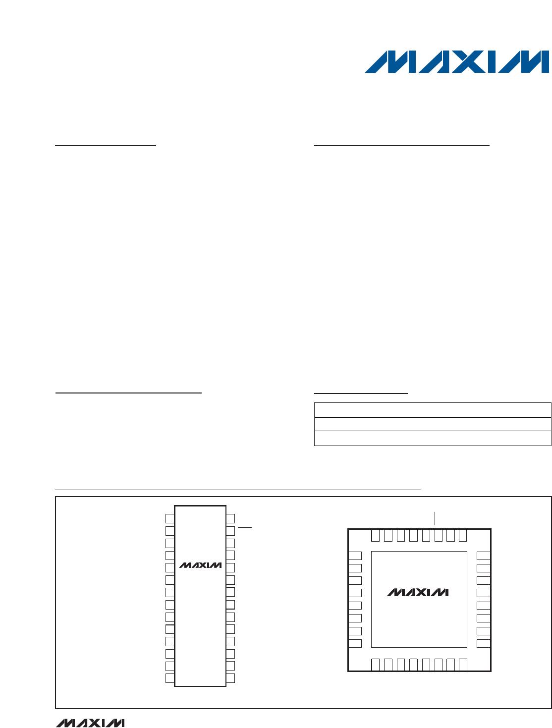
The MAX7033 is available in 28-pin TSSOP and
32-pin TQFN packages and is specified over the
extended (-40°C to +105°C) temperature range.
Features
o Optimized for 315MHz or 433MHz Band
o Operates from Single +3.3V or +5.0V Supplies
o High Dynamic Range with On-Chip AGC
o AGC Hold Circuit
o 1ms AGC Release Time
o Selectable Image-Rejection Center Frequency
o Selectable x64 or x32 f
LO
/f
XTAL
Ratio
o Low 5.2mA Operating Supply Current
o < 3.5µA Low-Current Power-Down Mode for
Efficient Power Cycling
o 250µs Startup Time
o Built-In 44dB RF Image Rejection
o Better than -114dBm Receive Sensitivity
o -40°C to +105°C Operation
MAX7033
315MHz/433MHz ASK Superheterodyne
Receiver with AGC Lock
________________________________________________________________
Maxim Integrated Products
1
28
27
26
25
24
23
22
21
20
19
18
17
16
15
1
2
3
4
5
6
7
8
9
10
11
12
13
14
XTAL2
SHDN
PDOUT
DATAOUT
V
DD5
DSP
AC
DFFB
OPP
DSN
DFO
IFIN2
IFIN1
XTALSEL
DVDD
DGND
MIXOUT
IRSEL
AGND
MIXIN2
MIXIN1
AVDD
LNAOUT
AGND
LNASRC
LNAIN
AVDD
XTAL1
TSSOP
TQFN
TOP VIEW
MAX7033
32
31
30
29
28
27
26
LNASRC
LNAIN
AVDD
XTAL1
XTAL2
SHDN
PDOUT
25 N.C.
9
10
11
12
13
14
15
MIXOUT
DGND
DVDD
AC
N.C.
XTALSEL
IFIN1
16IFIN2
17
18
19
20
21
22
23
DFO
DSN
OPP
DFFB
N.C.
DSP
V
DD5
8
7
6
5
4
3
2
IRSEL
AGND
MIXIN2
MIXIN1
AVDD
LNAOUT
AGND
MAX7033
1N.C.
24 DATAOUT
+
+
Pin Configurations
Ordering Information
Applications
19-3273; Rev 3; 9/11
For pricing, delivery, and ordering information, please contact Maxim Direct at 1-888-629-4642,
or visit Maxim’s website at www.maxim-ic.com.
+
Denotes a lead(Pb)-free/RoHS-compliant package.
*
EP = Exposed pad.
Typical Application Circuit appears at end of data sheet.
PART TEMP RANGE PIN-PACKAGE
MAX7033EUI+ -40°C to +105°C 28 TSSOP
MAX7033ETJ+ -40°C to +105°C 32 TQFN-EP*
Automotive Remote
Keyless Entry
Security Systems
Garage Door Openers
Home Automation
Remote Controls
Local Telemetry
Wireless Sensors
MAX7033
315MHz/433MHz ASK Superheterodyne
Receiver with AGC Lock
2 _______________________________________________________________________________________
ABSOLUTE MAXIMUM RATINGS
DC ELECTRICAL CHARACTERISTICS (+3.3V OPERATION)
(
Typical Application Circuit
, V
AVDD
= V
DVDD
= V
DD5
= +3.0V to +3.6V, no RF signal applied, T
A
= -40°C to +105°C, unless otherwise
noted. Typical values are at V
AVDD
= V
DVDD
= V
DD5
= +3.3V and T
A
= +25°C.) (Note 1)
Stresses beyond those listed under “Absolute Maximum Ratings” may cause permanent damage to the device. These are stress ratings only, and functional
operation of the device at these or any other conditions beyond those indicated in the operational sections of the specifications is not implied. Exposure to
absolute maximum rating conditions for extended periods may affect device reliability.
V
DD5
to AGND.......................................................-0.3V to +6.0V
AVDD to AGND .....................................................-0.3V to +4.0V
DVDD to DGND .....................................................-0.3V to +4.0V
AGND to DGND.....................................................-0.1V to +0.1V
IRSEL, DATAOUT, XTALSEL,
AC, SHDN to AGND .............................-0.3V to (V
DD5
+ 0.3V)
All Other Pins to AGND ..........................-0.3V to (V
DVDD
+ 0.3V)
Continuous Power Dissipation (T
A
= +70°C)
28-Pin TSSOP (derate 12.8mW/°C above +70°C) ..1025.6mW
32-Thin QFN (derate 21.3mW/°C above +70°C) ....1702.1mW
Operating Temperature Range .........................-40°C to +105°C
Junction Temperature......................................................+150°C
Storage Temperature Range .............................-60°C to +150°C
Lead Temperature (soldering 10s) ..................................+300°C
Soldering Temperature (reflow) .......................................+260°C
PARAMETER SYMBOL CONDITIONS MIN TYP MAX UNITS
Supply Voltage
V
AVDD
,
V
DVDD
+3.3V nominal supply voltage 3.0 3.3 3.6 V
f
RF
= 315MHz 5.2 6.23
Supply Current I
DD
V
SHDN
= V
DVDD
f
RF
= 433MHz 5.7 6.88
mA
f
RF
= 315MHz 2.6
Shutdown Supply Current I
SHDN
V
SHDN
= 0V,
V
XTALSEL
= 0V
f
RF
= 433MHz 3.5 8.0
μA
Input-Voltage Low V
IL
0.4 V
Input-Voltage High V
IH
V
DVDD
- 0.4
V
Input Logic Current High I
IH
10 μA
f
RF
= 433MHz, V
IRSEL
= V
DD5
V
DD5
-
0.4
f
RF
= 375MHz, V
IRSEL
= V
DD5
/2 1.1
V
DD5
-
1.0
Image-Reject Select Voltage
(Note 2)
f
RF
= 315MHz, V
IRSEL
= 0V 0.4
V
DATAOUT Output-Voltage Low V
OL
I
SINK
= 10μA 0.125 V
DATAOUT Output-Voltage High V
OH
I
SOURCE
= 10μA
V
DVDD
- 0.125
V
DC ELECTRICAL CHARACTERISTICS (+5.0V OPERATION)
(
Typical Application Circuit
, V
DD5
= +4.5V to +5.5V, no RF signal applied, T
A
= -40°C to +105°C, unless otherwise noted. Typical
values are at V
DD5
= +5.0V and T
A
= +25°C.) (Note 1)
PARAMETER SYMBOL CONDITIONS MIN TYP MAX UNITS
Supply Voltage V
DD5
+5.0V nominal supply voltage 4.5 5.0 5.5 V
f
RF
= 315MHz 5.2 6.4
Supply Current I
DD
V
SHDN
= V
DD5
f
RF
= 433MHz 5.7 6.76
mA
f
RF
= 315MHz 3.7
Shutdown Supply Current I
SHDN
V
SHDN
= 0V,
V
XTALSEL
= 0V
f
RF
= 433MHz 4.2 9.8
μA
Input-Voltage Low V
IL
0.4 V
MAX7033
315MHz/433MHz ASK Superheterodyne
Receiver with AGC Lock
_______________________________________________________________________________________ 3
DC ELECTRICAL CHARACTERISTICS (+5.0V OPERATION) (continued)
(
Typical Application Circuit
, V
DD5
= +4.5V to +5.5V, no RF signal applied, T
A
= -40°C to +105°C, unless otherwise noted. Typical
values are at V
DD5
= +5.0V and T
A
= +25°C.) (Note 1)
PARAMETER SYMBOL CONDITIONS MIN TYP MAX UNITS
Input-Voltage High V
IH
V
DD5
-
0.4
V
Input Logic Current High I
IH
15 μA
f
RF
= 433MHz, V
IRSEL
= V
DD5
V
DD5
-
0.4
f
RF
= 375MHz, V
IRSEL
= V
DD5
/2 1.1
V
DD5
-
1.5
Image-Reject Select Voltage
(Note 2)
f
RF
= 315MHz, V
IRSEL
= 0V 0.4
V
DATAOUT Output-Voltage Low V
OL
I
SINK
= 10μA 0.125 V
DATAOUT Output-Voltage High V
OH
I
SOURCE
= 10μA
V
DD5
-
0.125
V
AC ELECTRICAL CHARACTERISTICS
(
Typical Application Circuit
, V
AVDD
= V
DVDD
= V
DD5
= +3.0V to +3.6V, all RF inputs are referenced to 50Ω, f
RF
= 315MHz,
T
A
= -40°C to +105°C, unless otherwise noted. Typical values are at V
AVDD
= V
DVDD
= V
DD5
= +3.3V and T
A
= +25°C.) (Note 1)
PARAMETER SYMBOL CONDITIONS MIN TYP MAX UNITS
GENERAL CHARACTERISTICS
Startup Time t
ON
Time for valid signal detection after V
SHDN
= V
DVDD
250 μs
Receiver Input Frequency f
RF
300 450 MHz
Maximum Receiver Input Level Modulation depth >18dB 0 dBm
Average carrier power level -120
Sensitivity (Note 3)
Peak power level -114
dBm
LNA gain from low to high 8 dB
AGC Hysteresis
Switching time from low to high gain 1 ms
Manchester coded 33
Maximum Data Rate
NRZ coded 66
kbps
LNA IN HIGH-GAIN MODE
f
RF
= 433MHz 1 - j3.4
f
RF
= 375MHz 1 - j3.9Input Impedance Z
IN_LNA
Normalized to 50Ω
f
RF
= 315MHz 1 - j4.7
1dB Compression Point P1dB
LNA
-22 dBm
Input-Referred 3rd-Order
Intercept
IIP3
LNA
-12 dBm
LO Signal Feedthrough to
Antenna
-80 dBm
Noise Figure NF
LNA
3dB

MAX7033ETJ+

Mfr. #:
Manufacturer:
Maxim Integrated
Description:
RF Receiver 315MHz/433MHz ASK Superheterodyne Rec
Lifecycle:
New from this manufacturer.
Delivery:
DHL FedEx Ups TNT EMS
Payment:
T/T Paypal Visa MoneyGram Western Union

Products related to this Datasheet