Intermediate Frequency and RSSI
The IF section presents a differential 330Ω load to pro-
vide matching for the off-chip ceramic filter. The six
internal AC-coupled limiting amplifiers produce an
overall gain of approximately 65dB, with a bandpass-fil-
ter-type response centered near the 10.7MHz IF fre-
quency with a 3dB bandwidth of approximately 10MHz.
The RSSI circuit demodulates the IF by producing a DC
output proportional to the log of the IF signal level, with
a slope of approximately 14.2mV/dB (see the
Typical
Operating Characteristics
).
Applications Information
Crystal Oscillator
The crystal oscillator in the MAX7033 is designed to
present a capacitance of approximately 3pF between
the XTAL1 and XTAL2. If a crystal designed to oscillate
with a different load capacitance is used, the crystal is
pulled away from its stated operating frequency, intro-
ducing an error in the reference frequency. Crystals
designed to operate with higher differential load capac-
itance always pull the reference frequency higher. For
example, a 4.7547MHz crystal designed to operate
with a 10pF load capacitance oscillates at 4.7563MHz
with the MAX7033, causing the receiver to be tuned to
315.1MHz rather than 315.0MHz, an error of about
100kHz, or 320ppm.
In actuality, the oscillator pulls every crystal. The crys-
tal’s natural frequency is really below its specified fre-
quency, but when loaded with the specified load
capacitance, the crystal is pulled and oscillates at its
specified frequency. This pulling is already accounted
for in the specification of the load capacitance.
Additional pulling can be calculated if the electrical
parameters of the crystal are known. The frequency
pulling is given by:
where:
f
P
is the amount the crystal frequency pulled in ppm.
C
M
is the motional capacitance of the crystal.
C
CASE
is the case capacitance.
C
SPEC
is the specified load capacitance.
C
LOAD
is the actual load capacitance.
When the crystal is loaded as specified, i.e., C
LOAD
=
C
SPEC
, the frequency pulling equals zero.
It is possible to use an external reference oscillator in
place of a crystal to drive the VCO. AC-couple the exter-
nal oscillator to XTAL2 with a 1000pF capacitor. Drive
XTAL2 with a signal level of approximately -10dBm. AC-
couple XTAL1 to ground with a 1000pF capacitor.
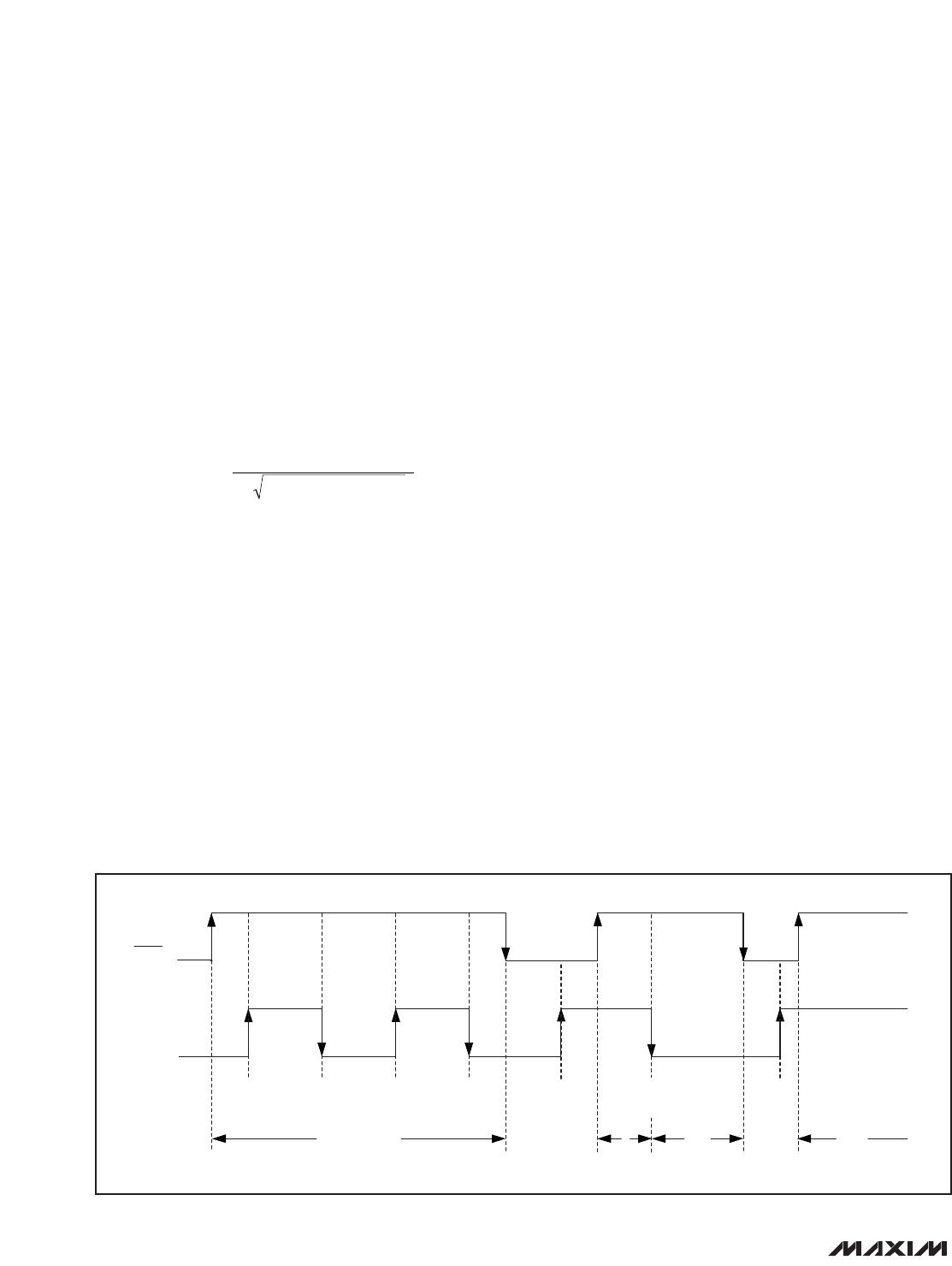
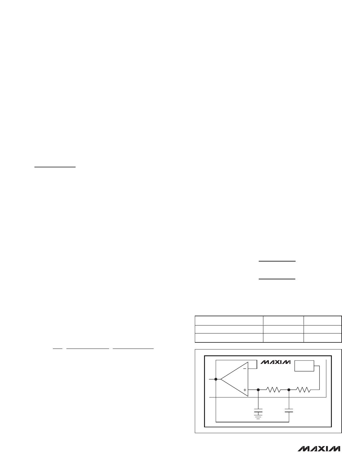
Data Filter
The data filter is implemented as a 2nd-order lowpass
Sallen-Key filter. The pole locations are set by the com-
bination of two on-chip resistors and two external
capacitors. Adjusting the value of the external capaci-
tors changes the corner frequency to optimize for dif-
ferent data rates. The corner frequency should be set
to approximately 1.5 times the fastest expected data
rate from the transmitter. Keeping the corner frequency
near the data rate rejects any noise at higher frequen-
cies, resulting in an increase in receiver sensitivity.
The configuration shown in Figure 2 can create a
Butterworth or Bessel response. The Butterworth filter
offers a very flat amplitude response in the passband
and a rolloff rate of 40dB/decade for the two-pole filter.
The Bessel filter has a linear phase response, which
works well for filtering digital data. To calculate the
value of C5 and C6, use the following equations, along
with the coefficients in Table 2:
where f
C
is the desired 3dB corner frequency.