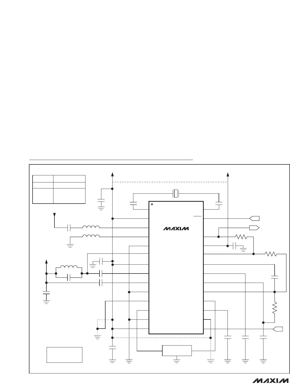
For example, to choose a Butterworth filter response
with a corner frequency of 5kHz:
Choosing standard capacitor values changes C5 to
470pF and C6 to 220pF, as shown in the
Typical
Application Circuit
.
Data Slicer
The data slicer takes the analog output of the data filter
and converts it to a digital signal. This is achieved by
using a comparator and comparing the analog input to
a threshold voltage. One input is supplied by the data
filter output. Both comparator inputs are accessible off-
chip to allow for different methods of generating the
slicing threshold, which is applied to the second com-
parator input.
The suggested data slicer configuration uses a resistor
(R1) connected between DSN and DSP with a capaci-
tor (C4) from DSN to DGND (Figure 3). This configura-
tion averages the analog output of the filter and sets the
threshold to approximately 50% of that amplitude. With
this configuration, the threshold automatically adjusts
as the analog signal varies, minimizing the possibility
for errors in the digital data. The values of R1 and C4
affect how fast the threshold tracks to the analog ampli-
tude. Be sure to keep the corner frequency of the RC
circuit much lower than the lowest expected data rate.
Note that a long string of zeros or ones can cause the
threshold to drift. This configuration works best if a cod-
ing scheme, such as Manchester coding, which has an
equal number of zeros and ones, is used.
To prevent continuous toggling of DATAOUT in the
absence of an RF signal due to noise, add hysteresis to
the data slicer as shown in Figure 4.
Peak Detector
The peak-detector output (PDOUT), in conjunction with
an external RC filter, creates a DC output voltage equal
to the peak value of the data signal. The resistor pro-
vides a path for the capacitor to discharge, allowing the
peak detector to dynamically follow peak changes of
the data-filter output voltage. For faster data slicer
response, use the circuit shown in Figure 5.
C
k kHz
pF
C
k kHz
pF
5
1 000
1 414 100 3 14 5
450
6
1 414
4 100 3 14 5
225
.
..
.
.
=
()( )()()
=
()( )( )( )
Ω
Ω
MAX7033
315MHz/433MHz ASK Superheterodyne
Receiver with AGC Lock
______________________________________________________________________________________ 13
DATA
SLICER
R1
25
DATAOUT
20
DSN
19
DFO
23
DSP
C4
MAX7033
Figure 3. Generating Data Slicer Threshold
DATA
SLICER
R3
R1
R2
R4
25
DATAOUT
*OPTIONAL
23
DSP
19
DFO
20
DSN
C4
MAX7033
Figure 4. Generating Data Slicer Hysteresis
DATA
SLICER
25kΩ
25
DATAOUT
20
DSN
19
DFO
26
PDOUT
23
DSP
MAX7033
47nF
Figure 5. Using PDOUT for Faster Startup
MAX7033
315MHz/433MHz ASK Superheterodyne
Receiver with AGC Lock
14 ______________________________________________________________________________________
Typical Application Circuit
28
C13
L1
C11
C1
C2
L2
L3
C3
C4
V
DD3
RF INPUT
V
DD3
V
DD
C12
X1
27
26
25
24
23
22
21
20
19
18
17
16
15
1
2
3
4
5
6
7
8
9
10
11
12
13
14
MAX7033
DVDD
IF FILTER
COMPONENT VALUES
IN TABLE 1
**SEE THE
MIXER
SECTION. *SEE
PHASE-LOCKED LOOP
SECTION.
Y1
*
**
GND
IN OUT
DGND
MIXOUT
IRSEL
AGND
MIXIN2
MIXIN1
AVDD
LNAOUT
C9
C10
AGND
LNASRC
LNAIN
AVDD
XTAL1 XTAL2
TO/FROM μP
POWER-DOWN
DATA OUT
SHDN
PDOUT
DATAOUT
V
DD5
DSP
AC
DFFB
C8
R1
FROM μP
R2
R3
C7
C6C5
OPP
DSN
DFO
IFIN2
IFIN1
XTALSEL
IF V
DD
IS
3.0V TO 3.6V
THEN V
DD3
IS
CONNECTED TO V
DD
CREATED BY LDO,
AVAILABLE AT AVDD
(PIN 2)
C15
C14
(SEE TABLE)
4.5V TO 5.5V
Layout Considerations
A properly designed PCB is an essential part of any
RF/microwave circuit. On high-frequency inputs and
outputs, use controlled-impedance lines and keep
them as short as possible to minimize losses and radia-
tion. At high frequencies, trace lengths that are on the
order of λ/10 or longer act as antennas.
Keeping the traces short also reduces parasitic induc-
tance. Generally, 1in of a PCB trace adds about 20nH
of parasitic inductance. The parasitic inductance can
have a dramatic effect on the effective inductance of a
passive component. For example, a 0.5in trace con-
necting a 100nH inductor adds an extra 10nH of induc-
tance or 10%.
To reduce the parasitic inductance, use wider traces
and a solid ground or power plane below the signal
traces. Also, use low-inductance connections to
ground on all GND pins, and place decoupling capaci-
tors close to all power-supply pins.
Control Interface Considerations
When operating the MAX7033 with a +4.5V to +5.5V
supply voltage, the SHDN and AC pins can be driven
by a microcontroller with either 3V or 5V interface logic
levels. When operating the MAX7033 with a +3.0V to
+3.6V supply, only 3V logic from the microcontroller is
allowed.
MAX7033
Chip Information
PROCESS: CMOS
315MHz/433MHz ASK Superheterodyne
Receiver with AGC Lock
______________________________________________________________________________________ 15
Package Information
For the latest package outline information and land patterns
(footprints), go to www.maxim-ic.com/packages. Note that a
“+”, “#”, or “-” in the package code indicates RoHS status only.
Package drawings may show a different suffix character, but
the drawing pertains to the package regardless of RoHS status.
PACKAGE
TYPE
PACKAGE
CODE
OUTLINE NO.
LAND
PATTERN NO.
28 TSSOP U28+1
21-0066
90-0171
32 TQFN-EP T3255+3
21-0140
90-0001

MAX7033ETJ+

Mfr. #:
Manufacturer:
Maxim Integrated
Description:
RF Receiver 315MHz/433MHz ASK Superheterodyne Rec
Lifecycle:
New from this manufacturer.
Delivery:
DHL FedEx Ups TNT EMS
Payment:
T/T Paypal Visa MoneyGram Western Union

Products related to this Datasheet