MARCH 3, 2017 19 PROGRAMMABLE CLOCK GENERATOR
5P49V5901 DATASHEET
Table 22:PCI Express Jitter Specifications (V
DDO
= 3.3V+5% or 2.5V+5%, T
A
= -40°C to +85°C)
Note: Electrical parameters are guaranteed over the specified ambient operating temperature range, which is established when the device is mounted in a test
socket with maintained transverse airflow greater than 500 lfpm. The device will meet specifications after thermal equilibrium has been reached under these
conditions.
1. Peak-to-Peak jitter after applying system transfer function for the Common Clock Architecture. Maximum limit for PCI Express Gen 1.
2. RMS jitter after applying the two evaluation bands to the two transfer functions defined in the Common Clock Architecture and reporting the worst case results
for each evaluation band. Maximum limit for PCI Express Generation 2 is 3.1ps RMS for t
REFCLK_HF_RMS
(High Band) and 3.0ps RMS for t
REFCLK_LF_RMS
(Low
Band).
3. RMS jitter after applying system transfer function for the common clock architecture. This specification is based on the PCI_Express_Base_r3.0 10 Nov, 2010
specification, and is subject to change pending the final release version of the specification.
4. This parameter is guaranteed by characterization. Not tested in production.
Table 23:Jitter Specifications
1,2,3
Symbol Parameter Conditions Min Typ Max PCIe Industry
Specification
Units Notes
t
J
(PCIe Gen1)
Phase Jitter
Peak-to-Peak
ƒ = 100MHz, 25MHz Crystal Input
Evaluation Band: 0Hz - Nyquist
(clock frequency/2)
30 86 ps 1,4
t
REFCLK_HF_RMS
(PCIe Gen2) Phase Jitter RMS
ƒ = 100MHz, 25MHz Crystal Input
High Band: 1.5MHz - Nyquist (clock
frequency/2)
2.56 3.10 ps 2,4
t
REFCLK_LF_RMS
(PCIe Gen2)
Phase Jitter RMS
ƒ = 100MHz, 25MHz Crystal Input
Low Band: 10kHz - 1.5MHz
0.27 3.0 ps 2,4
t
REFCLK_RMS
(PCIe Gen3) Phase Jitter RMS
ƒ = 100MHz, 25MHz Crystal Input
Evaluation Band: 0Hz - Nyquist
(clock frequency/2)
0.8 1.0 ps 3,4
Parameter Symbol Test Condition Min Typ Max Unit
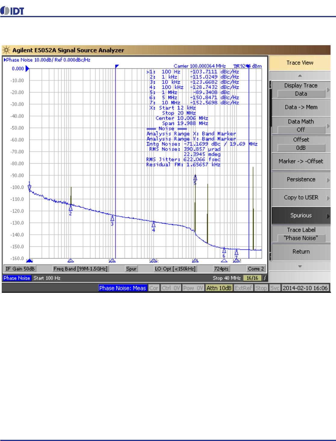
GbE Random Jitter (12 kHz–20 MHz)
4
J
GbE
Crystal in = 25 MHz, All CLKn at 125 MHz
5
- 0.79 0.95 ps
GbE Random Jitter (1.875–20 MHz) R
JGbE
Crystal in = 25 MHz, All CLKn at 125 MHz
5
- 0.32 0.5 ps
OC-12 Random Jitter (12 kHz–5 MHz) J
OC12
CLKIN = 19.44 MHz, All CLKn at 155.52 MHz
5
- 0.69 0.95 ps
PCI Express 1.1 Common Clocked
Total Jitter
6
- 9.1 12 ps
RMS Jitter
6
, 10 kHz to 1.5MHz - 0.1 0.3 ps
RMS Jitter
6
, 1.5MHz to 50MHz - 0.9 1.1 ps
PCI Express 3.0 Common Clocked
RMS Jitter
6
-0.20.4ps
2
For best jitter performance, keep the single ended clock input slew rates at more than 1.0 V/ns and the differential clock input slew rates more than 0.3 V/ns.
3
All jitter data in this table is based upon all output formats being diff erential. When single-ended outputs are used, there is the potential that the output jitter may increase
due to the nature of single-ended outputs. If your configuration implements any single-ended output and any output is required to have jitter less than 3 ps rms, contact
IDT for support to validate your configuration and ensure the best jitter performance. In many configurations, CMOS outputs have little to no effect upon jitter.
4
DJ for PCI and GbE is < 5 ps pp.
5
Output FOD in Integer mode.
6
All output clocks 100 MHz HCSL format. Jitter is from the PCIE jitter filter combination that produces the highest jitter. Jitter is measured w ith the Intel Clock Jitter Tool,
Ver. 1.6.6.
PCI Express 2.1 Common Clocked
(VDDx = 3.3V+5% or 2.5V+5%, TA = -40°C to +85°C)
1
All measurements w ith Spread Spectrum Off.
Notes :