MARCH 3, 2017 25 PROGRAMMABLE CLOCK GENERATOR
5P49V5901 DATASHEET
LVPECL Driver
Figure General Diagram for LVPECL Driver to XTAL Input
Interface shows an example of the interface diagram for a
+3.3V LVPECL driver. This is a standard LVPECL termination
with one side of the driver feeding the XIN/REF input. It is
recommended that all components in the schematics be
placed in the layout; though some components might not be
used, they can be utilized for debugging purposes. The
datasheet specifications are characterized and guaranteed by
using a quartz crystal as the input. If the driver is 2.5V
LVPECL, the only change necessary is to use the appropriate
value of R3.
General Diagram for +3.3V LVPECL Driver to XTAL Input Interface
CLKIN Equivalent Schematic
Figure CLKIN Equivalent Schematic below shows the basis of
the requirements on VIH max, VIL min and the 1200 mV p-p
single ended Vswing maximum.
The CLKIN and CLKINB Vih max spec comes from the
cathode voltage on the input ESD diodes D2 and D4, which
are referenced to the internal 1.2V supply. CLKIN or
CLKINB voltages greater than 1.2V + 0.5V =1.7V will be
clamped by these diodes. CLKIN and CLKINB input
voltages less than -0.3V will be clamped by diodes D1 and
D3.
The 1.2V p-p maximum Vswing input requirement is
determined by the internally regulated 1.2V supply for the
actual clock receiver. This is the basis of the Vswing spec in
Table 13.
+3 .3V LV PE CL Dr iv er
Zo = 50 Ohm
Zo = 50 Ohm
R1
50
R2
50
R3
50
XOUT
XIN / REF
C1
0. 1 uF
PROGRAMMABLE CLOCK GENERATOR 26 MARCH 3, 2017
5P49V5901 DATASHEET
CLKIN Equivalent Schematic
Wiring the Differential Input to Accept Single-Ended Levels
Figure Recommended Schematic for Wiring a Differential
Input to Accept Single-ended Levels
shows how a differential
input can be wired to accept single ended levels. This
configuration has three properties; the total output impedance
of Ro and Rs matches the 50 ohm transmission line
impedance, the Vrx voltage is generated at the CLKIN inputs
which maintains the LVCMOS driver voltage level across the
transmission line for best S/N and the R1-R2 voltage divider
values ensure that Vrx p-p at CLKIN is less than the maximum
value of 1.2V.
Recommended Schematic for Wiring a Differential Input to Accept Single-ended Levels
R1
R2
Vrx
VersaClock 5 Receiver
CLKI N
CLKI NB
LV CMOS
VDD
Zo = 50 Ohm
Ro + Rs = 50
Rs
Ro
MARCH 3, 2017 27 PROGRAMMABLE CLOCK GENERATOR
5P49V5901 DATASHEET
Table 26 Nominal Voltage Divider Values vs Driver VDD
shows resistor values that ensure the maximum drive level for
the CLKIN port is not exceeded for all combinations of 5%
tolerance on the driver VDD, the VersaClock Vddo_0 and 5%
resistor tolerances. The values of the resistors can be
adjusted to reduce the loading for slower and weaker
LVCMOS driver by increasing the impedance of the R1-R2
divider. To assist this assessment, the total load on the driver
is included in the table.
Table 26: Nominal Voltage Divider Values vs Driver VDD
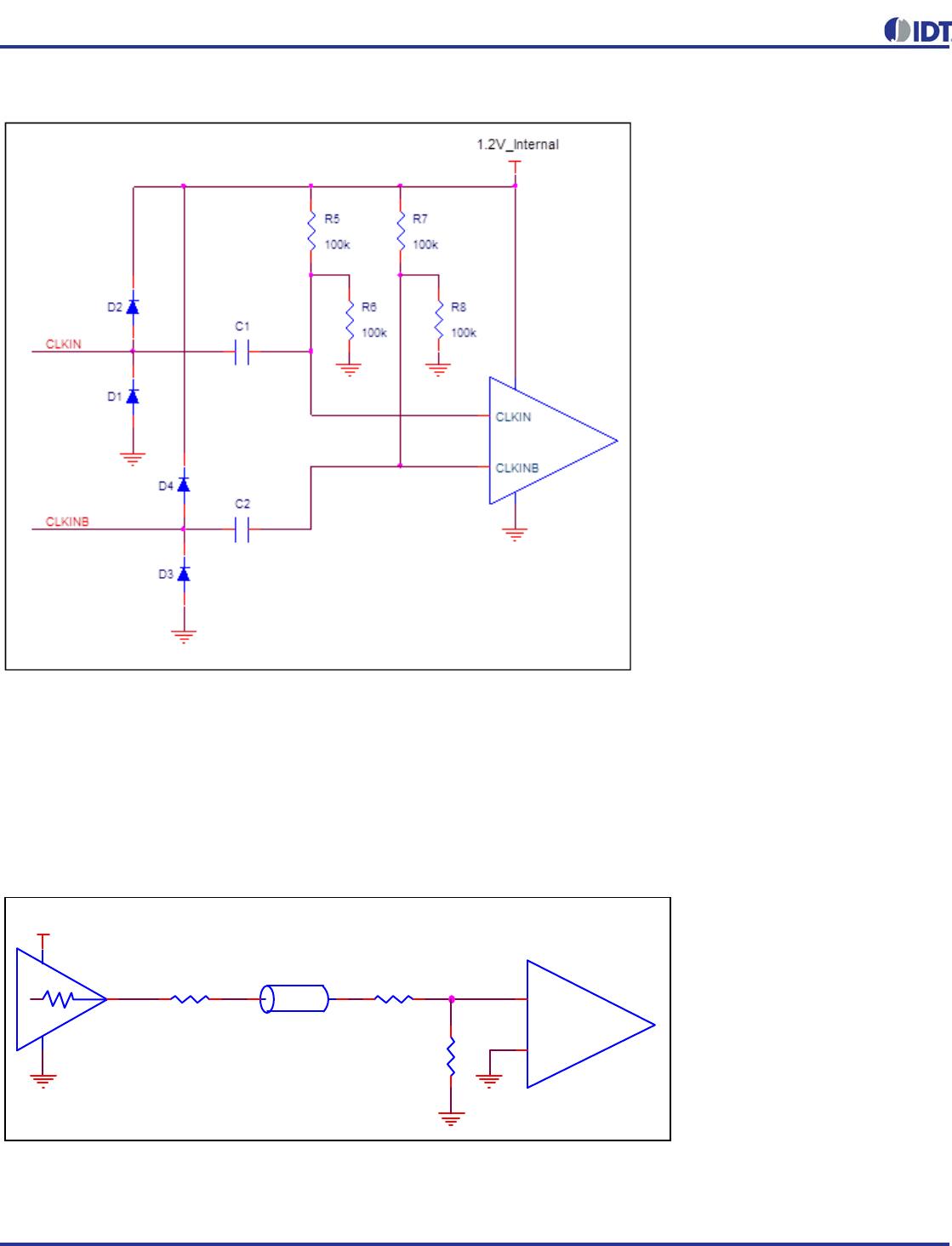
HCSL Differential Clock Input Interface
CLKIN/CLKINB will accept DC coupled HCSL signals.
CLKIN, CLKINB Input Driven by an HCSL Driver
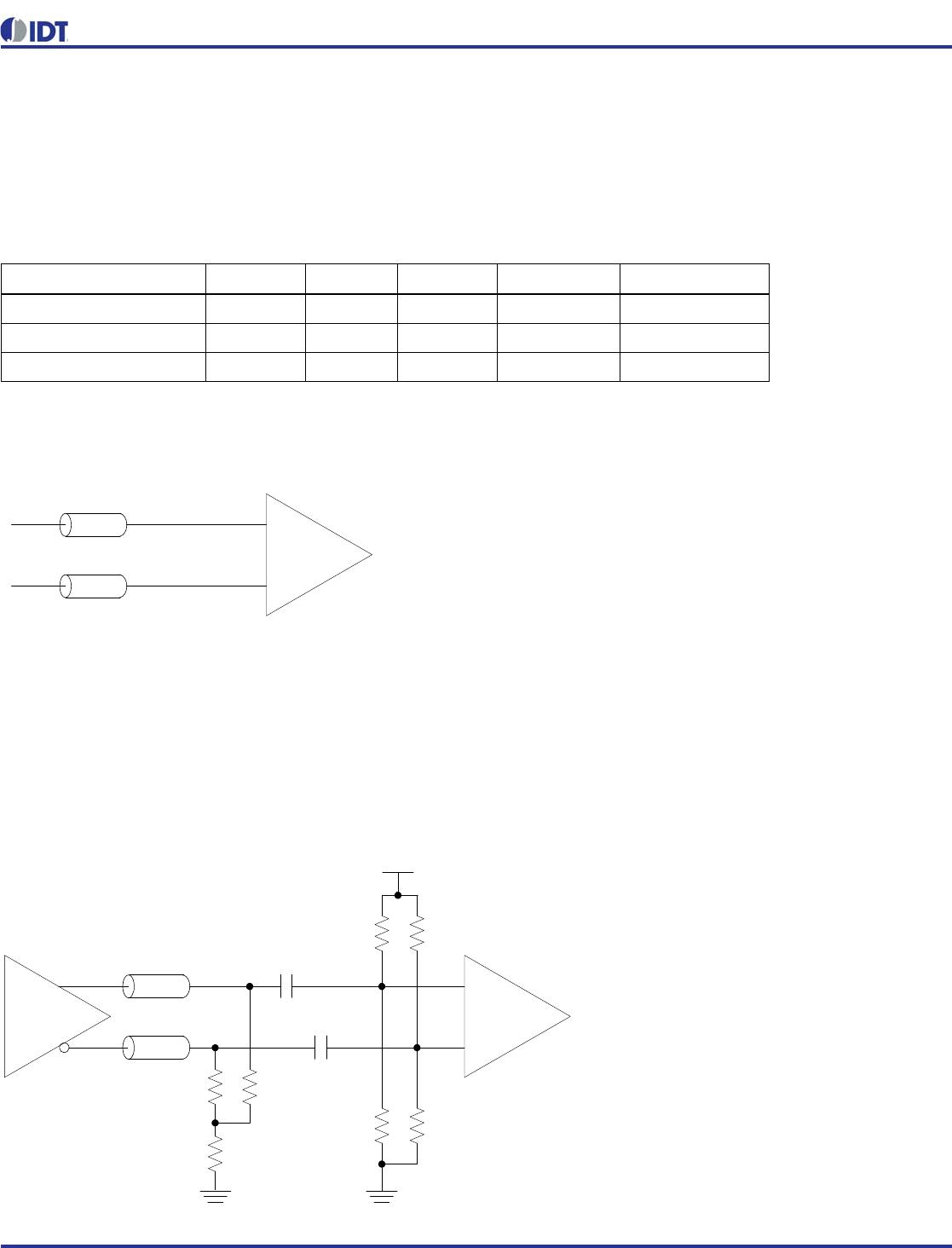
3.3V Differential LVPECL Clock Input Interface
The logic levels of 3.3V LVPECL and LVDS can exceed VIH
max for the CLKIN/B pins. Therefore the LVPECL levels must
be AC coupled to the VersaClock differential input and the DC
bias restored with external voltage dividers. A single table of
bias resistor values is provided below for both for 3.3V
LVPECL and LVDS. Vbias can be VDDD, V
DDOX
or any other
available voltage at the VersaClock receiver that is most
conveniently accessible in layout.
CLKIN, CLKINB Input Driven by a 3.3V LVPECL Driver
LVCMOS Driver VDD Ro+Rs R1 R2 Vrx (peak) Ro+Rs+R1+R2
3.3 50.0 130 75 0.97 255
2.5 50.0 100 100 1.00 250
1.8 50.0 62 130 0.97 242
Zo=50ohm
Zo=50ohm
CLKIN
CLKINB
VersaClock 5 Receiver
Q
nQ
+3.3V LVPECL
Driver
Zo=50ohm
Zo=50ohm
VersaClock 5 Receiver
R9 R10
50ohm
50ohm
Vbias
Rpu1 Rpu2
CLKIN
CLKINB
RTT
50ohm
C5
0.01µF
C6
0.01µF
R15
4.7kohm
R13
4.7kohm

5P49V5901B045NLGI8

Mfr. #:
Manufacturer:
IDT
Description:
Clock Generators & Support Products VersaClock 5 CLK Gen 350MHz 2 Input
Lifecycle:
New from this manufacturer.
Delivery:
DHL FedEx Ups TNT EMS
Payment:
T/T Paypal Visa MoneyGram Western Union