REF19x Series Data Sheet
Rev. L | Page 16 of 28
ABSOLUTE MAXIMUM RATINGS
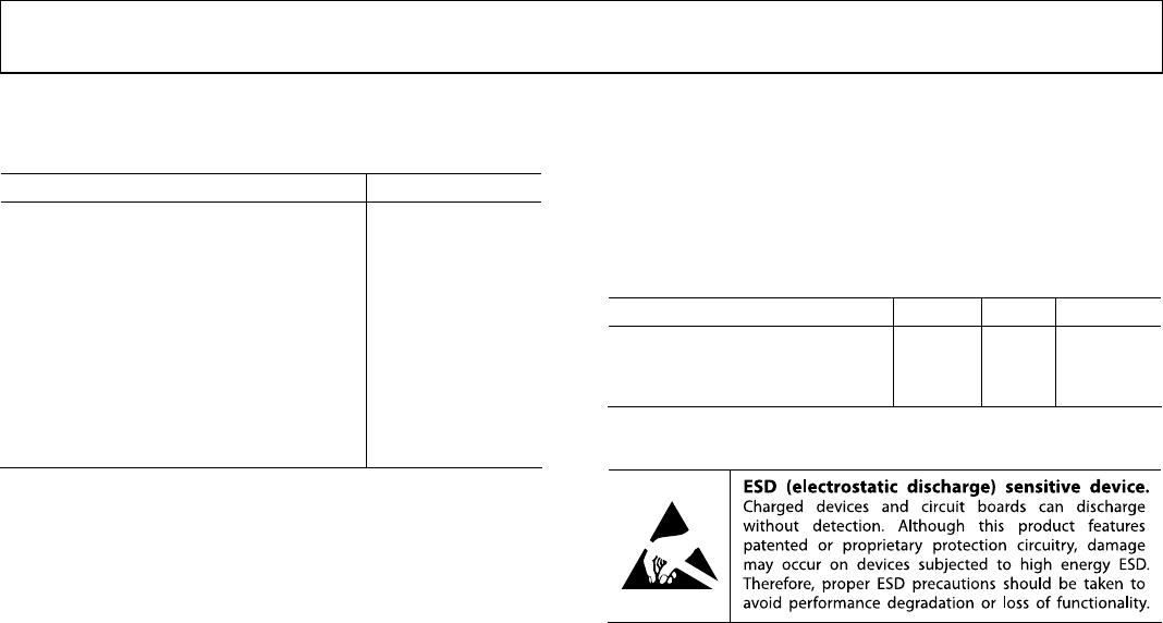
Table 23.
Parameter Rating
Supply Voltage −0.3 V to +18 V
Output to GND −0.3 V to V
S
+ 0.3 V
Output to GND Short-Circuit Duration Indefinite
Storage Temperature Range
PDIP, SOIC Package −65°C to +150°C
Operating Temperature Range
REF19x −40°C to +125°C
Junction Temperature Range
PDIP, SOIC Package −65°C to +150°C
Lead Temperature (Soldering 60 sec) 300°C
Stresses above those listed under Absolute Maximum Ratings
may cause permanent damage to the device. This is a stress
rating only; functional operation of the device at these or any
other conditions above those indicated in the operational
section of this specification is not implied. Exposure to absolute
maximum rating conditions for extended periods may affect
device reliability.
THERMAL RESISTANCE
θ
JA
is specified for worst-case conditions; that is, θ
JA
is specified
for the device in socket for PDIP and is specified for the device
soldered in the circuit board for the SOIC and TSSOP packages.
Table 24.
Package Type θ
JA
θ
JC
Unit
8-Lead PDIP (N) 103 43 °C/W
8-Lead SOIC (R) 158 43 °C/W
8-Lead TSSOP (RU) 240 43 °C/W
ESD CAUTION
Data Sheet REF19x Series
Rev. L | Page 17 of 28
TYPICAL PERFORMANCE CHARACTERISTICS
00371-003
TEMPERATURE (°C)
100–50 –25 0 25 50 75
OUTPUT VOLTAGE (V)
5.004
5.003
5.001
5.002
5.000
4.999
4.998
4.997
4.996
3 TYPICAL PARTS
5.15V
<
V
IN
<
15V
Figure 3. REF195 Output Voltage vs. Temperature
00371-004
I
LOAD
(mA)
300 5 10 15 20 25
LOAD REGULATION (ppm/V)
32
24
28
20
16
12
4
8
0
–40°C
+25°C
5.15V V
S
15V
+85°C
Figure 4. REF195 Load Regulator vs. I
LOAD
V
IN
(V)
1646 8 101214
LINE REGUL
A
TION (ppm/mA)
20
16
12
8
4
0
+85°C
+25°C
–40°C
0mA I
OUT
25mA
00371-005
Figure 5. REF195 Line Regulator vs. V
IN
T
C
V
OUT
(ppm/°C)
20–20 –10–15 0–5 10 155
PERCENTAGE OF PARTS
50
45
40
30
35
20
25
10
5
15
0
BASED ON 600
UNITS, 4 RUNS
–40°C T
A
+85°C
00371-006
Figure 6. T
C
V
OUT
Distribution
00371-007
TEMPERATURE (°C)
100–50 –25 0 25 50 75
SUPPLY CURRENT (
μ
A)
40
35
30
25
20
15
10
5
0
NORMAL MODE
SLEEP MODE
Figure 7. Supply Current vs. Temperature
TEMPERATURE (°C)
10050250 255075
SLEEP PIN CURRENT (µA)
6
–5
–4
–3
–1
–2
0
V
L
V
H
00371-008
Figure 8.
SLEEP
Pin Current vs. Temperature
REF19x Series Data Sheet
Rev. L | Page 18 of 28
00371-009
FREQUENCY (Hz)
1M10 100 1k 10k 100k
RIPPLE REJECTION (dB)
–20
0
–60
–40
–80
–120
–100
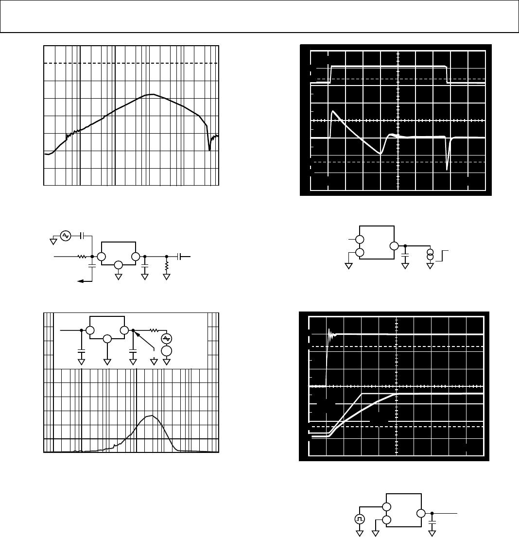
Figure 9. Ripple Rejection vs. Frequency
REF19x
1kΩ
REF
10μF
V
IN
= 15V
OUTPUT
1kΩ
10μF
1μF10μF
2 6
4
00371-010
Figure 10. Ripple Rejection vs. Frequency Measurement Circuit
00371-011
FREQUENCY (Hz)
10M10 100 10k1k 100k 1M
Z
O
(Ω)
4
3
2
1
0
V
G
= 2V p-p
V
S
= 4V
V
IN
= 7V 200V
1μF1μF
REF19x
2 6
4
Z
Figure 11. Output Impedance vs. Frequency
O
FF
ON
100µs20mV
5V
10%
0%
90%
100%
00371-012
Figure 12. Load Transient Response
V
IN
= 15V
0
10mA
1μF
REF19x
4
2
6
00371-013
Figure 13. Load Transient Response Measurement Circuit
2V
2V
1mA
LOAD
30mA
LOAD
100µs
10%
100%
0%
90%
00371-014
Figure 14. Power-On Response Time
V
IN
= 7V
1μF
REF19x
4
2
6
00371-015
Figure 15. Power-On Response Time Measurement Circuit

REF191ESZ-REEL

Mfr. #:
Manufacturer:
Analog Devices Inc.
Description:
Voltage References 2.048V Prec Micropwr LDO Low VRef
Lifecycle:
New from this manufacturer.
Delivery:
DHL FedEx Ups TNT EMS
Payment:
T/T Paypal Visa MoneyGram Western Union