REF19x Series Data Sheet
Rev. L | Page 22 of 28
management should still be exercised. A short, heavy, low dc
resistance (DCR) conductor should be used from U1 to 6 to the V
OUT
Sense Point S, where the collector of Q1 connects to the load, Point F.
Because of the current limiting configuration, the dropout voltage
circuit is raised about 1.1 V over that of the REF19x devices, due to
the V
BE
of Q1 and the drop across Current Sense Resistor R4.
However, overall dropout is typically still low enough to allow
operation of a 5 V to 3.3 V regulator/reference using the REF196 for
U1 as noted, with a V
S
as low as 4.5 V and a load current of 150 mA.
The requirement for a heat sink on Q1 depends on the maximum
input voltage and short-circuit current. With V
S
= 5 V and a
300 mA current limit, the worst-case dissipation of Q1 is 1.5 W,
less than the TO-220 package 2 W limit. However, if smaller TO-39
or TO-5 package devices, such as the 2N4033, are used, the current
limit should be reduced to keep maximum dissipation below
the package rating. This is accomplished by simply raising R4.
A tantalum output capacitor is used at C1 for its low equivalent
series resistance (ESR), and the higher value is required for stability.
Capacitor C2 provides input bypassing and can be an ordinary
electrolytic.
Shutdown control of the booster stage is an option, and when used,
some cautions are needed. Due to the additional active devices
in the V
S
line to U1, a direct drive to Pin 3 does not work as with an
unbuffered REF19x device. To enable shutdown control, the
connection from U1 to Q2 is broken at the X, and Diode D1
then allows a CMOS control source, V
C
, to drive U1 to 3 for on/off
operation. Startup from shutdown is not as clean under heavy
load as it is in basic REF19x series, and can require several
milliseconds under load. Nevertheless, it is still effective and
can fully control 150 mA loads. When shutdown control is
used, heavy capacitive loads should be minimized.
NEGATIVE PRECISION REFERENCE WITHOUT
PRECISION RESISTORS
In many current-output CMOS DAC applications where the output
signal voltage must be the same polarity as the reference voltage, it
is often necessary to reconfigure a current-switching DAC into
a voltage-switching DAC using a 1.25 V reference, an op amp,
and a pair of resistors. Using a current-switching DAC directly
requires an additional operational amplifier at the output to
reinvert the signal. A negative voltage reference is then desirable
because an additional operational amplifier is not required for
either reinversion (current-switching mode) or amplification
(voltage-switching mode) of the DAC output voltage. In general,
any positive voltage reference can be converted into a negative
voltage reference using an operational amplifier and a pair of
matched resistors in an inverting configuration. The disadvantage
to this approach is that the largest single source of error in the
circuit is the relative matching of the resistors used.
The circuit illustrated in Figure 26 avoids the need for tightly
matched resistors by using an active integrator circuit. In this
circuit, the output of the voltage reference provides the input
drive for the integrator. To maintain circuit equilibrium, the
integrator adjusts its output to establish the proper relationship
between the V
OUT
and GND references. Thus, any desired negative
output voltage can be selected by substituting for the appropriate
reference IC. The sleep feature is maintained in the circuit with
the simple addition of a PNP transistor and a 10 kΩ resistor.
100
1µF
1k
1µF
–V
REF
REF19x
V
S
GND
OUTPUT
100k
SLEEP
TTL/CMOS
A1 = 1/2 OP295,
1/2 OP291
V
S
10k
2N3906
3 6
2
4
SLEEP
10k
+5V
–5V
A1
00371-024
Figure 26. Negative Precision Voltage Reference Uses No Precision Resistors
One caveat to this approach is that although rail-to-rail output
amplifiers work best in the application, these operational amplifiers
require a finite amount (mV) of headroom when required to provide
any load current; consider this issue when choosing the negative
supply for the circuit.
STACKING REFERENCE ICs FOR ARBITRARY
OUTPUTS
Some applications may require two reference voltage sources that
are a combined sum of standard outputs. The circuit in Figure 27
shows how this stacked output reference can be implemented.
Two reference ICs are used, fed from a common unregulated input,
V
S
. The outputs of the individual ICs are connected in series, as
shown in Figure 27, which provide two output voltages, V
OUT1
and
V
OUT2
. V
OUT1
is the terminal voltage of U1, whereas V
OUT2
is the
sum of this voltage and the terminal voltage of U2. U1 and U2
are chosen for the two voltages that supply the required outputs
(see Table 1). If, for example, both U1 and U2 are REF192s, the
two outputs are 2.5 V and 5.0 V.
R1
3.9k
(SEE TEXT)
C1
0.1µF
+V
S
V
S
> V
OUT2
+ 0.15V
V
IN
COMMON
V
OUT
COMMON
OUTPUT TABLE
U1/U2
REF192/REF192
REF192/REF194
REF192/REF195
V
OUT1
(V)
2.5
2.5
2.5
V
OUT2
(V)
5.0
7.0
7.5
+V
OUT2
C2
1µF
C3
0.1µF
+V
OUT1
C4
1µF
U2
REF19x
(SEE TABLE)
2
63
4
U1
REF19x
(SEE TABLE)
2
63
4
+
+
V
O
(U2)
V
O
(U1)
00371-025
Figure 27. Stacking Voltage References with the REF19x
Data Sheet REF19x Series
Rev. L | Page 23 of 28
Although this concept is simple, some cautions are needed. Because
the lower reference circuit must sink a small bias current from U2
(50 μA to 100 μA), plus the base current from the series PNP output
transistor in U2, either the external load of U1 or R1 must provide
a path for this current. If the U1 minimum load is not well defined,
Resistor R1 should be used, set to a value that conservatively passes
600 μA of current with the applicable V
OUT1
across it. Note that the
two U1 and U2 reference circuits are locally treated as macrocells,
each having its own bypasses at input and output for best stability.
Both U1 and U2 in this circuit can source dc currents up to
their full rating. The minimum input voltage, V
S
, is determined by
the sum of the outputs, V
OUT2
, plus the dropout voltage of U2.
A related variation on stacking two 3-terminal references is shown
in Figure 28, where U1, a REF192, is stacked with a 2-terminal
reference diode, such as the AD589. Like the 3-terminal stacked
reference shown in Figure 27, this circuit provides two outputs,
V
OUT1
and V
OUT2
, which are the individual terminal voltages of D1
and U1, respectively. Here this is 1.235 V and 2.5 V, which provides a
V
OUT2
of 3.735 V. When using 2-terminal reference diodes, such as
D1, the rated minimum and maximum device currents must be
observed, and the maximum load current from V
OUT1
can be no
greater than the current setup by R1 and V
O
(U1). When V
O
(U1) is equal to 2.5 V, R1 provides a 500 μA bias to D1, so the
maximum load current available at V
OUT1
is 450 μA or less.
D1
AD589
R1
4.99kΩ
(SEE TEXT)
C1
0.1μF
+V
S
V
S
> V
OUT2
+ 0.15V
V
IN
COMMON
V
OUT
COMMON
+V
OUT2
3.735V
C2
1μF
+V
OUT1
1.235V
C3
1μF
U1
REF192
2
63
4
+
+
V
O
(U1)
V
O
(D1)
00371-026
Figure 28. Stacking Voltage References with the REF192
PRECISION CURRENT SOURCE
In low power applications, the need often arises for a precision
current source that can operate on low supply voltages. As
shown in Figure 29, any one of the devices in the REF19x family
of references can be configured as a precision current source.
The circuit configuration illustrated is a floating current source
with a grounded load. The output voltage of the reference is
bootstrapped across R
SET
, which sets the output current into the
load. With this configuration, circuit precision is maintained for
load currents in the range from the references supply current
(typically 30 μA) to approximately 30 mA. The low dropout
voltage of these devices maximizes the current sources output
voltage compliance without excess headroom.
I
SY
ADJUST
R1
R
SET
P1
R
L
I
OUT
FOR EXAMPLE, REF195: V
OUT
= 5V
I
OUT
= 5mA
R1 = 953
P1 = 100, 10-TURN
V
S
1µF
REF19x
2
3
4
6
V
IN
I
OUT
× R
L
(MAX) + V
SY
(MIN)
I
OUT
=
V
OUT
+ I
SY
(REF19x)
R
SET
V
OUT
>> I
SY
R
SET
V
S
GND
OUTPUTSLEEP
00371-027
Figure 29. A Low Dropout, Precision Current Source
SWITCHED OUTPUT 5 V/3.3 V REFERENCE
Applications often require digital control of reference voltages,
selecting between one stable voltage and a second. With the
sleep feature inherent to the REF19x series, switched output
reference configurations are easily implemented with little
additional hardware.
The circuit in Figure 30 shows the general technique, which takes
advantage of the output wire-OR capability of the REF19x device
family. When off, a REF19x device is effectively an open circuit
at the output node with respect to the power supply. When on, a
REF19x device can source current up to its current rating, but
sink only a few μA (essentially, just the relatively low current of the
internal output scaling divider). Consequently, when two devices
are wired together at their common outputs, the output voltage
is the same as the output voltage for the on device. The off state
device draws a small standby current of 15 μA (maximum), but
otherwise does not interfere with operation of the on device, which
can operate to its full current rating. Note that the two devices in
the circuit conveniently share both input and output capacitors,
and with CMOS logic drive, it is power efficient.
U3B
74HC04
U3A
74HC04
V
C
V
OUT
(V)
5.0
3.3
4.5
5.0
V
C
*
HIGH
LOW
HIGH
LOW
U1/U2
REF195/
REF196
REF194/
REF195
*
CMOS LOGIC LEVELS
+V
S
= 6V
V
IN
COMMON
V
OUT
COMMON
C1
0.1µF
+V
OUT
C2
1µF
U1
REF19x
(SEE TABLE)
2
3
4
U2
REF19x
(SEE TABLE)
2
3
4
+
6
6
1324
OUTPUT T
A
BLE
00371-028
Figure 30. Switched Output Reference
REF19x Series Data Sheet
Rev. L | Page 24 of 28
2
3
1
+V
OUT
SENSE
+V
OUT
FORCE
R
LW
1µF 100k
R
L
REF19x
V
S
GND
OUTPUT
A1 = 1/2 OP295
1/2 OP292
OP183
V
S
6
2
4
SLEEP
V
S
R
LW
A1
3
00371-029
Using dissimilar REF19x series devices with this configuration
allows logic selection between the U1/U2-specified terminal
voltages. For example, with U1 (a REF195) and U2 (a REF196),
as noted in the table in Figure 30, changing the CMOS-compatible
V
C
logic control voltage from high to low selects between a nominal
output of 5.0 V and 3.3 V, and vice versa. Other REF19x family
units can also be used for U1/U2, with similar operation in a
logic sense, but with outputs as per the individual paired devices
(see the table in Figure 30). Of course, the exact output voltage
tolerance, drift, and overall quality of the reference voltage is
consistent with the grade of individual U1 and U2 devices.
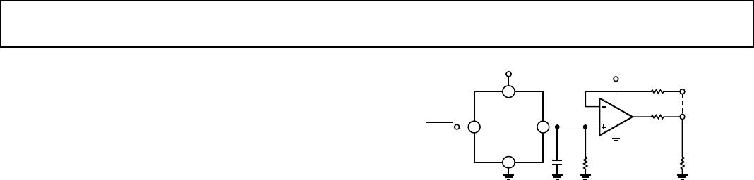
Figure 31. Low Dropout, Kelvin-Connected Voltage Reference
FAIL-SAFE 5 V REFERENCE
Some critical applications require a reference voltage to be
maintained at a constant voltage, even with a loss of primary
power. The low standby power of the REF19x series and the
switched output capability allow a fail-safe reference con-
figuration to be implemented rather easily. This reference
maintains a tight output voltage tolerance for either a primary
power source (ac line derived) or a standby (battery derived)
power source, automatically switching between the two as the
power conditions change.
Due to the nature of the wire-OR, one application caveat should
be understood about this circuit. Because U1 and U2 can only
source current effectively, negative going output voltage changes,
which require the sinking of current, necessarily take longer than
positive going changes. In practice, this means that the circuit is
quite fast when undergoing a transition from 3.3 V to 5 V, but the
transition from 5 V to 3.3 V takes longer. Exactly how much
longer is a function of the load resistance, R
L
, seen at the output and
the typical 1 μF value of C2. In general, a conservative transition
time is approximately several milliseconds for load resistances
in the range of 100 Ω to 1 kΩ. Note that for highest accuracy at
the new output voltage, several time constants should be allowed
(for example, >7.6 time constants for <1/2 LSB error @ 10 bits).
The circuit in Figure 32 illustrates this concept, which borrows
from the switched output idea of Figure 30, again using the
REF19x device family output wire-OR capability. In this case,
because a constant 5 V reference voltage is desired for all condi-
tions, two REF195 devices are used for U1 and U2, with their
on/off switching controlled by the presence or absence of the
primary dc supply source, V
S
. V
BAT
is a 6 V battery backup
source that supplies power to the load only when V
S
fails. For
normal (V
S
present) power conditions, V
BAT
sees only the 15 μA
(maximum) standby current drain of U1 in its off state.
KELVIN CONNECTIONS
In many portable applications where the PCB cost and area go
hand-in-hand, circuit interconnects are very often narrow. These
narrow lines can cause large voltage drops if the voltage reference is
required to provide load currents to various functions. The inter-
connections of a circuit can exhibit a typical line resistance of
0.45 mΩ/square (for example, 1 oz. Cu).
In operation, it is assumed that for all conditions, either U1 or
U2 is on, and a 5 V reference output is available. With this
voltage constant, a scaled down version is applied to the
Comparator IC U3, providing a fixed 0.5 V input to the negative
input for all power conditions. The R1 to R2 divider provides a
signal to the U3 positive input proportionally to V
S
, which
switches U3 and U1/U2, dependent upon the absolute level of
V
S
. In Figure 32, Op Amp U3 is configured as a comparator
with hysteresis, which provides clean, noise-free output
switching. This hysteresis is important to eliminate rapid
switching at the threshold due to V
S
ripple. Furthermore, the
device chosen is the AD820, a rail-to-rail output device. This
device provides high and low output states within a few mV of
V
S
, ground for accurate thresholds, and compatible drive for U2
for all V
S
conditions. R3 provides positive feedback for circuit
hysteresis, changing the threshold at the positive input as a
function of the output of U3.
In applications where these devices are configured as low dropout
voltage regulators, these wiring voltage drops can become a large
source of error. To circumvent this problem, force and sense
connections can be made to the reference through the use of an
operational amplifier, as shown in Figure 31. This method provides
a means by which the effects of wiring resistance voltage drops can
be eliminated. Load currents flowing through wiring resistance
produce an I-R error (I
LOAD
× R
WIRE
) at the load. However, the
Kelvin connection overcomes the problem by including the
wiring resistance within the forcing loop of the op amp. Because
the op amp senses the load voltage, op amp loop control forces
the output to compensate for the wiring error and to produce
the correct voltage at the load. Depending on the reference
device chosen, operational amplifiers that can be used in this
application are the OP295, OP292, and OP183.

REF191ESZ-REEL

Mfr. #:
Manufacturer:
Analog Devices Inc.
Description:
Voltage References 2.048V Prec Micropwr LDO Low VRef
Lifecycle:
New from this manufacturer.
Delivery:
DHL FedEx Ups TNT EMS
Payment:
T/T Paypal Visa MoneyGram Western Union