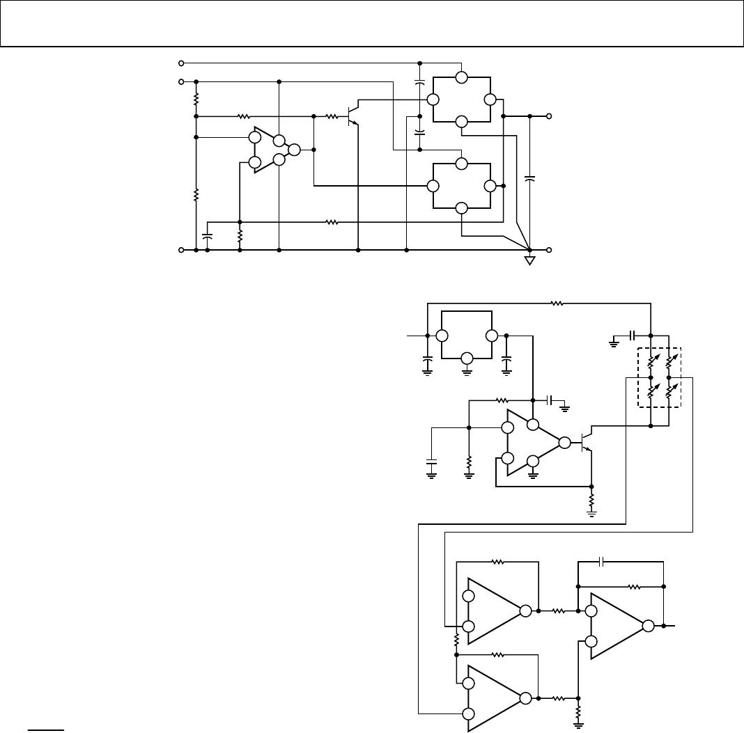
Data Sheet REF19x Series
Rev. L | Page 27 of 28
ORDERING GUIDE
Model
1
Temperature Range Package Description Package Option Ordering Quantity
REF191ES −40°C to +85°C 8-Lead SOIC_N S-Suffix (R-8)
REF191ES-REEL −40°C to +85°C 8-Lead SOIC_N S-Suffix (R-8) 2,500
REF191ESZ −40°C to +85°C 8-Lead SOIC_N S-Suffix (R-8)
REF191ESZ-REEL −40°C to +85°C 8-Lead SOIC_N S-Suffix (R-8) 2,500
REF191GS −40°C to +85°C 8-Lead SOIC_N S-Suffix (R-8)
REF191GS-REEL −40°C to +85°C 8-Lead SOIC_N S-Suffix (R-8) 2,500
REF191GSZ −40°C to +85°C 8-Lead SOIC_N S-Suffix (R-8)
REF191GSZ-REEL −40°C to +85°C 8-Lead SOIC_N S-Suffix (R-8) 2,500
REF192ES −40°C to +85°C 8-Lead SOIC_N S-Suffix (R-8)
REF192ES-REEL −40°C to +85°C 8-Lead SOIC_N S-Suffix (R-8) 2,500
REF192ES-REEL7 −40°C to +85°C 8-Lead SOIC_N S-Suffix (R-8) 1,000
REF192ESZ −40°C to +85°C 8-Lead SOIC_N S-Suffix (R-8)
REF192ESZ-REEL −40°C to +85°C 8-Lead SOIC_N S-Suffix (R-8) 2,500
REF192ESZ-REEL7 −40°C to +85°C 8-Lead SOIC_N S-Suffix (R-8) 1,000
REF192FS −40°C to +85°C 8-Lead SOIC_N S-Suffix (R-8)
REF192FS-REEL −40°C to +85°C 8-Lead SOIC_N S-Suffix (R-8) 2,500
REF192FS-REEL7 −40°C to +85°C 8-Lead SOIC_N S-Suffix (R-8) 1,000
REF192FSZ −40°C to +85°C 8-Lead SOIC_N S-Suffix (R-8)
REF192FSZ-REEL −40°C to +85°C 8-Lead SOIC_N S-Suffix (R-8) 2,500
REF192FSZ-REEL7 −40°C to +85°C 8-Lead SOIC_N S-Suffix (R-8) 1,000
REF192GPZ −40°C to +85°C 8-Lead PDIP P-Suffix (N-8)
REF192GRUZ −40°C to +85°C 8-Lead TSSOP RU-8
REF192GRUZ-REEL7 −40°C to +85°C 8-Lead TSSOP RU-8 1,000
REF192GS −40°C to +85°C 8-Lead SOIC_N S-Suffix (R-8)
REF192GS-REEL −40°C to +85°C 8-Lead SOIC_N S-Suffix (R-8) 2,500
REF192GS-REEL7 −40°C to +85°C 8-Lead SOIC_N S-Suffix (R-8) 1,000
REF192GSZ −40°C to +85°C 8-Lead SOIC_N S-Suffix (R-8)
REF192GSZ-REEL −40°C to +85°C 8-Lead SOIC_N S-Suffix (R-8) 2,500
REF192GSZ-REEL7 −40°C to +85°C 8-Lead SOIC_N S-Suffix (R-8) 1,000
REF193GSZ −40°C to +85°C 8-Lead SOIC_N S-Suffix (R-8)
REF193GSZ-REEL −40°C to +85°C 8-Lead SOIC_N S-Suffix (R-8) 2,500
REF194ES −40°C to +85°C 8-Lead SOIC_N S-Suffix (R-8)
REF194ESZ −40°C to +85°C 8-Lead SOIC_N S-Suffix (R-8)
REF194ESZ-REEL −40°C to +85°C 8-Lead SOIC_N S-Suffix (R-8) 2,500
REF194GS-REEL −40°C to +85°C 8-Lead SOIC_N S-Suffix (R-8) 2,500
REF194GS-REEL7 −40°C to +85°C 8-Lead SOIC_N S-Suffix (R-8) 1,000
REF194GSZ −40°C to +85°C 8-Lead SOIC_N S-Suffix (R-8)
REF194GSZ-REEL −40°C to +85°C 8-Lead SOIC_N S-Suffix (R-8) 2,500
REF194GSZ-REEL7 −40°C to +85°C 8-Lead SOIC_N S-Suffix (R-8) 1,000
REF195ES −40°C to +85°C 8-Lead SOIC_N S-Suffix (R-8)
REF195ES-REEL −40°C to +85°C 8-Lead SOIC_N S-Suffix (R-8) 2,500
REF195ESZ −40°C to +85°C 8-Lead SOIC_N S-Suffix (R-8)
REF195ESZ-REEL −40°C to +85°C 8-Lead SOIC_N S-Suffix (R-8) 2,500
REF195FS −40°C to +85°C 8-Lead SOIC_N S-Suffix (R-8)
REF195FS-REEL −40°C to +85°C 8-Lead SOIC_N S-Suffix (R-8) 2,500
REF195FSZ −40°C to +85°C 8-Lead SOIC_N S-Suffix (R-8)
REF195FSZ-REEL −40°C to +85°C 8-Lead SOIC_N S-Suffix (R-8) 2,500
REF195GPZ −40°C to +85°C 8-Lead PDIP P-Suffix (N-8)
REF195GRU-REEL7 −40°C to +85°C 8-Lead TSSOP RU-8 1,000
REF195GRUZ −40°C to +85°C 8-Lead TSSOP RU-8
REF195GRUZ-REEL7 −40°C to +85°C 8-Lead TSSOP RU-8 1,000