LTC4219
1
4219fd
For more information www.linear.com/LTC4219
Typical applicaTion
FeaTures
applicaTions
DescripTion
5A Integrated
Hot Swap Controller
The LT C
®
4219 is an integrated solution for Hot Swap
applications that allows a board to be safely inserted and
removed from a live backplane. The part integrates a Hot
Swap controller, power MOSFET and current sense resis
-
tor in a single package for small form factor applications.
The LTC4219
provides separate inrush current control
and a 10% accurate 5.6A current limit with foldback cur
-
rent limiting. The current limit threshold can be adjusted
dynamically using an external pin. Additional features
include a current monitor output that amplifies the sense
resistor voltage for ground referenced current sensing
and a MOSFET temperature monitor output. Thermal limit
and power good monitoring are also provided. The power
good detection level and foldback current limit profile are
internally preset for 5V (LTC4219-5) and 12V (LTC4219-12)
applications.
L, LT , LT C , LT M , Linear Technology and the Linear logo are registered trademarks of Linear
Technology Corporation. All other trademarks are the property of their respective owners.
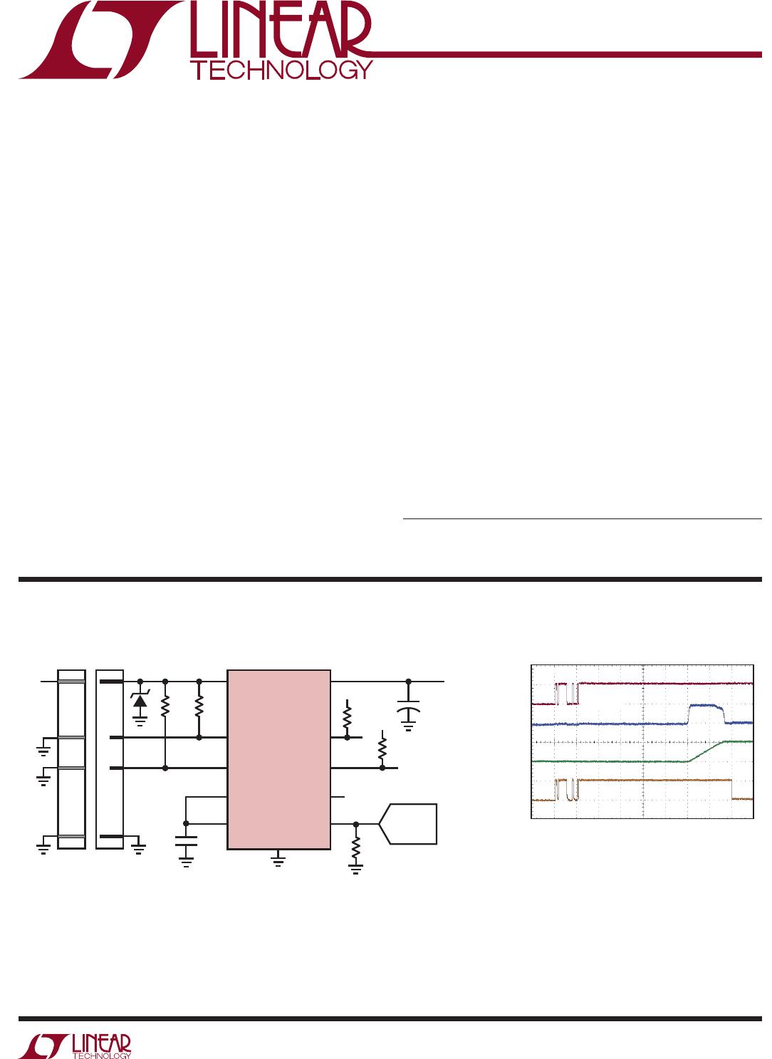
12V, 5A Card Resident Application
n
Small Footprint
n
33mΩ MOSFET with R
SENSE
n
Available in Preset 12V and 5V Versions
n
Adjustable, 10% Accurate Current Limit
n
Current and Temperature Monitor Outputs
n
Overtemperature Protection
n
Adjustable Current Limit Timer Before Fault
n
Power Good and Fault Outputs
n
Adjustable Inrush Current Control
n
Available in 16-Lead 5mm × 3mm DFN Package
n
RAID Systems
n
Server I/O Cards
n
Industrial
Power-Up Waveforms
12V
V
OUT
12V
5A
4219 TA01a
330µF
10k
V
DD
TIMER
INTV
CC
OUT
PG
GND
F LT
I
SET
I
MON
LTC4219DHC-12
EN2
EN1
+
20k
F
*TVS: DIODES INC. SMAJ17A
10k
ADC
12V
12V
200k200k
*
V
IN
10V/DIV
I
IN
0.1A/DIV
V
OUT
10V/DIV
PG
10V/DIV
20ms/DIV
CONTACT
BOUNCE
4219 TA01b
LTC4219
2
4219fd
For more information www.linear.com/LTC4219
16
15
14
13
12
11
10
9
17
SENSE
1
2
3
4
5
6
7
8
V
DD
I
SET
I
MON
FB
F LT
PG
GATE
OUT
V
DD
EN1
EN2
TIMER
INTV
CC
GND
OUT
OUT
TOP VIEW
DHC PACKAGE
16-LEAD (5mm × 3mm) PLASTIC DFN
T
JMAX
= 125°C, q
JA
= 43°C/W
q
JA
= 43°C/W EXPOSED PAD SOLDERED, OTHERWISE q
JA
= 140°C/W
orDer inFormaTion
absoluTe maximum raTings
Supply Voltage (V
DD
) ................................. 0.3V to 28V
Input Voltages
FB,
EN1,
EN2 ...........................................0.3V to 12V
TIMER
................................................... 0.3V to 3.5V
SENSE
.............................V
DD
10V or – 0.3V to V
DD
Output Voltages
I
SET
, I
MON
................................................. 0.3V to 3V
PG, F
LT ................................................... 0.3V to 35V
OUT
............................................ 0.3V to V
DD
+ 0.3V
INTV
CC
.................................................. 0.3V to 3.5V
GATE (Note 3)
........................................ 0.3V to 33V
Operating Ambient Temperature Range
LTC4
219C
................................................ C to 70°C
LTC4219I
.............................................40°C to 8C
Junction Temperature (Notes 4, 5) ........................ 125°C
Storage Temperature Range .................. 65°C to 150°C
(Notes 1, 2)
pin conFiguraTion
LEAD FREE FINISH TAPE AND REEL PART MARKING* PACKAGE DESCRIPTION TEMPERATURE RANGE
LTC4219CDHC-12#PBF LTC4219CDHC-12#TRPBF 421912 16-Lead (5mm × 3mm) Plastic DFN 0°C to 70°C
LTC4219IDHC-12#PBF LTC4219IDHC-12#TRPBF 421912 16-Lead (5mm × 3mm) Plastic DFN –40°C to 85°C
LTC4219CDHC-5#PBF LTC4219CDHC-5#TRPBF 42195 16-Lead (5mm × 3mm) Plastic DFN 0°C to 70°C
LTC4219IDHC-5#PBF LTC4219IDHC-5#TRPBF 42195 16-Lead (5mm × 3mm) Plastic DFN –40°C to 85°C
Consult LTC Marketing for parts specified with wider operating temperature ranges. *The temperature grade is identified by a label on the shipping container.
For more information on lead free part marking, go to: http://www.linear.com/leadfree/
For more information on tape and reel specifications, go to: http://www.linear.com/tapeandreel/. Some packages are available in 500 unit reels through
designated sales channels with #TRMPBF suffix.
LTC4219
3
4219fd
For more information www.linear.com/LTC4219
elecTrical characTerisTics
The l denotes the specifications which apply over the full operating
temperature range, otherwise specifications are at T
A
= 25°C. V
DD
= 12V unless otherwise noted.
SYMBOL PARAMETER CONDITIONS MIN TYP MAX UNITS
DC Characteristics
V
DD
Input Supply Range
l
2.9 15 V
I
DD
Input Supply Current MOSFET On, No Load
l
1.6 3 mA
V
DD(UVL)
Input Supply Undervoltage Lockout V
DD
Rising
l
2.65 2.73 2.85 V
V
OUT(PGTH)
Output Power Good Threshold LTC4219-12, V
OUT
Rising
l
10.2 10.5 10.8 V
LTC4219-5, V
OUT
Rising
l
4.2 4.35 4.5 V
DV
OUT(PGHYST)
Output Power Good Hysteresis LTC4219-12
l
127 170 213 mV
LTC4219-5
l
53 71 89 mV
I
OUT
OUT Leakage Current V
OUT
= V
GATE
= 0V, V
DD
= 15V
l
0 ±150 µA
V
OUT
= V
GATE
= 12V, LTC4219-12
l
50 70 90 µA
V
OUT
= V
GATE
= 5V, LTC4219-5
l
26 36 46.5 µA
dV
GATE
/dt GATE Pin Turn-On Ramp Rate
l
0.15 0.3 0.55 V/ms
R
ON
MOSFET + Sense Resistor On Resistance
l
15 33 50 mW
I
LIM(TH)
Current Limit Threshold V
FB
= 1.23V
l
5.0 5.6 6.1 A
V
FB
= 0V
l
1.2 1.5 1.8 A
V
FB
= 1.23V, R
SET
= 20kΩ
l
2.6 2.9 3.3 A
Inputs
I
IN
EN1, EN2 Input Current V
PIN
= 1.2V
l
0 ±1 µA
R
FB
FB Input Resistance LTC4219-12
LTC4219-5
l
l
13
20
18
29
23
37
V
TH
EN1, EN2, FB Threshold Voltage V
PIN
Rising
l
1.21 1.235 1.26 V
DV
EN(HYST)
EN1, EN2 Hysteresis
l
50 80 110 mV
DV
FB(HYST)
FB Power Good Hysteresis
l
10 20 30 mV
R
ISET
I
SET
Internal Resistor
l
19 20 21
kW

LTC4219IDHC-5#TRPBF

Mfr. #:
Manufacturer:
Analog Devices Inc.
Description:
Hot Swap Voltage Controllers 5V, 5A Integrated Hot Swap Controller
Lifecycle:
New from this manufacturer.
Delivery:
DHL FedEx Ups TNT EMS
Payment:
T/T Paypal Visa MoneyGram Western Union