LTC4219
10
4219fd
For more information www.linear.com/LTC4219
operaTion
The Functional Diagram displays the main circuits of the
device. The LTC4219 is designed to turn a boards supply
voltage on and off in a controlled manner allowing the board
to be safely inserted and removed from a live backplane.
The LTC4219 includes a 25mW MOSFET and a 7.5mW
current sense resistor. During normal operation, the charge
pump and gate driver turn on the pass MOSFETs gate to
provide power to the load. The inrush current control is
accomplished by the INRUSH circuit. This circuit limits
the GATE ramp rate to 0.3V/ms and hence controls the
voltage ramp rate of the output capacitor.
The current sense (CS) amplifier monitors the load current
using the voltage sensed across the current sense resistor.
The CS amplifier limits the current in the load by reduc
-
ing the GATE-to-OUT voltage in an active control loop. It
is simple to adjust the current limit threshold using the
current limit adjustment
(I
SET
) pin. This allows a different
threshold during other times such as start-up.
A short circuit on the output to ground causes significant
power dissipation during active current limiting. To limit
this power, the foldback amplifier reduces the current
limit value from 5.6A to 1.5A in a linear manner as the
FB pin drops below 0.6V (see the Typical Performance
Characteristics section).
If an overcurrent condition persists, the TIMER pin ramps
up with a 100µA current source until the pin voltage
exceeds 1.235V (comparator TM2). This indicates to the
logic that it is time to turn off the pass MOSFET to prevent
overheating. At this point the TIMER pin ramps down us
-
ing the A current source until the voltage drops below
0.21V
(Comparator TM1) which tells the logic to start an
internal 100ms timer. After this delay, the pass transistor
has cooled and it is safe to turn it on again. It is suitable
for many applications to use an internal 2ms overcurrent
timer with a 100ms cooldown period. Tying the TIMER
pin to INTV
CC
sets this default timing.
The fixed 5V and 12V versions, LTC4219-5 and LTC4219-12,
use an internal divider from OUT to drive the FB pin. This
divider also sets the foldback current limit profile
.
The
output voltage is monitored using the FB pin and the PG
comparator to determine if the power is available for the
load. The power good condition is signaled by the PG pin
using an open-drain pull-down transistor.
The Functional Diagram also shows the monitoring blocks
of the LTC4219. The two comparators on the left side in
-
clude the EN
1 and EN2
comparators. These comparators
determine if the enable inputs are valid prior to turning on
the MOSFET. But first the undervoltage lockout circuits
UVLO1 and UVLO2 must validate the input supply and
the internally generated 3.1V supply (INTV
CC
) and gener-
ate the power up initialization to the logic circuits. If the
external conditions remain valid for 100
ms the MOSFET
is allowed to turn on.
Other features include MOSFET current and temperature
monitoring. The current monitor (CM) outputs a current
proportional to the sense resistor current. This current can
drive an external resistor or other circuits for monitoring
purposes. A voltage proportional to the MOSFET tempera
-
ture is output to the I
SET
pin. The MOSFET is protected by
a thermal shutdown circuit.
LTC4219
11
4219fd
For more information www.linear.com/LTC4219
applicaTions inFormaTion
This gate slope is designed to charge up a 1000µF capaci-
tor to 12V
in 40ms, with an inrush current of 300mA. This
allows the inrush current to stay under the current limit
threshold (1.5A) for capacitors less than 1000µF. Included
in the Typical Performance Characteristics section is a
graph of the Safe Operating Area for the MOSFET. It is
evident from this graph that the power dissipation at 12V,
300mA for 40ms is in the safe region.
Adding the R
GATE
, C
GATE
and C
COMP
network on the GATE
pin will lower the inrush current below the default value
set by the inrush circuit. The GATE is then charged with
a 24µA current source. The voltage at the GATE pin rises
with a slope equal to 24µA/C
GATE
and the supply inrush
current is set at:
I
INRUSH
=
C
L
C
GATE
24µA
Figure 2. Supply Turn-On
Figure 1. 2A, 12V Card Resident Application with Auto-Retry
The typical LTC4219 application is in a high availability
system that uses a positive voltage supply to distribute
power to individual cards. A complete application circuit
is shown in Figure 1. External component selection is
discussed in detail in the following sections.
Turn-On Sequence
Several conditions must be present before the internal
pass MOSFET can be turned on. First the supply V
DD
must
exceed its undervoltage lockout level. Next the internally
generated supply INTV
CC
must cross its 2.65V under-
voltage threshold. This generates a 25µs power-on-reset
pulse which clears the fault register and initializes internal
latches.
Finally, the enable inputs EN1 and EN2 both must
be below the 1.15V threshold. All of these conditions must
be satisfied for the duration of 100ms to ensure that any
contact bounce during the insertion has ended.
The MOSFET is turned on by charging up the GATE with
a charge pump generated 24µA current source whose
value is adjusted by shunting a portion of the pull-up cur
-
rent to ground. The charging current is controlled by the
INRUSH circuit that maintains a constant slope of GATE
voltage versus time (Figure 2). The voltage at the GATE
pin rises with a slope of 0.3[V/ms] and the supply inrush
current is set at:
I
INRUSH
= C
L
0.3[V/ms]
ADC
C1
F
12V
12V
PG = 10.5V
4219 F01
R4
10k
R1
10k
Q1
BSS84
C
T
0.1µF
C
L
330µF
C
COMP
3.3nF
V
OUT
12V
2A
V
DD
EN1
OUT
PG
GND
I
MON
R
SET
20k
R
MON
20k
I
SET
C
GATE
0.1µF
R
GATE
100k
GATE
LTC4219DHC-12
EN2
INTV
CC
TIMER
F LT
+
*TVS Z1: DIODES INC. SMAJ17A
R3
200k
R2
200k
R4 10k
Z1*
t1 t2
SLOPE = 0.3[V/ms]
GATE
OUT
V
DD
+ 6.15V
V
DD
4219 F02
LTC4219
12
4219fd
For more information www.linear.com/LTC4219
applicaTions inFormaTion
If V
DD
drops below 2.65V for greater than s or INTV
CC
drops below 2.5V for greater than 1µs, a fast shutdown
of the switch is initiated. The GATE is pulled down with a
140mA current to the OUT pin.
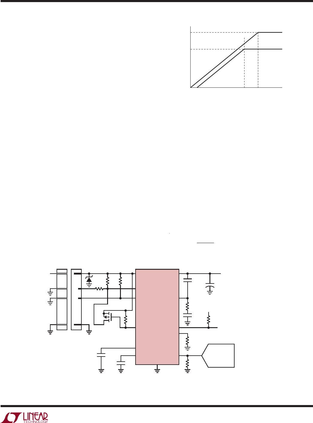
Overcurrent Fault
The LTC4219 features an adjustable current limit with
foldback that protects against short circuits and excessive
load current. To prevent excessive power dissipation in the
switch during active current limit, the available current is
reduced as a function of the output voltage sensed by the
FB pin. A graph in the Typical Performance Characteristics
curves shows the current limit versus FB voltage.
An overcurrent fault occurs when the current limit circuitry
has been engaged for longer than the time-out delay set
by the TIMER. Current limiting begins when the MOSFET
current reaches 1.5A to 5.6A (depending on the foldback).
The GATE pin is then brought down with a 140mA GATE-
to-OUT current. The voltage on the GATE is regulated in
order to limit the current to less than 5.6A. At this point,
a circuit breaker time delay starts by charging the external
timing capacitor with a 100µA pull-up current from the
TIMER pin. If the TIMER pin reaches its 1.235V threshold,
the internal switch turns off (with a 250µA current from
GATE to ground). Included in the Typical Performance
Characteristics curves is a graph of the Safe Operating
Area for the MOSFET. From this graph one can determine
the MOSFETs maximum time in current limit for a given
output power.
Tying the TIMER pin to INTV
CC
will force the part to use
the internally generated (circuit breaker) delay of 2ms.
In either case the F LT pin is pulled low to indicate an
overcurrent fault has turned off the pass MOSFET. For a
given circuit breaker time delay, the equation for setting
the timing capacitor’s value is as follows:
C
T
= t
CB
0.083[µF/ms]
After the switch is turned off, the TIMER pin begins
discharging the timing capacitor with a A pull-down
current. When the TIMER pin reaches its 0.21V threshold,
an internal 100ms timer is started. After the 100ms delay,
the switch is allowed to turn on again if the overcurrent
fault latch has been cleared. Bringing the EN1 pin above
When the GATE voltage reaches the MOSFET threshold
voltage, the switch begins to turn on and the OUT volt
-
age follows the GATE voltage as it increases. Once OUT
reaches V
DD
, the GATE will ramp up until clamped by the
6.15V Zener between GATE and OUT.
As the OUT voltage rises, so will the FB pin which is moni
-
toring it. Once the FB pin crosses its 1.235V threshold and
the GATE to OUT voltage exceeds 4.2V, the PG pin pulls
low indicating that the power is good.
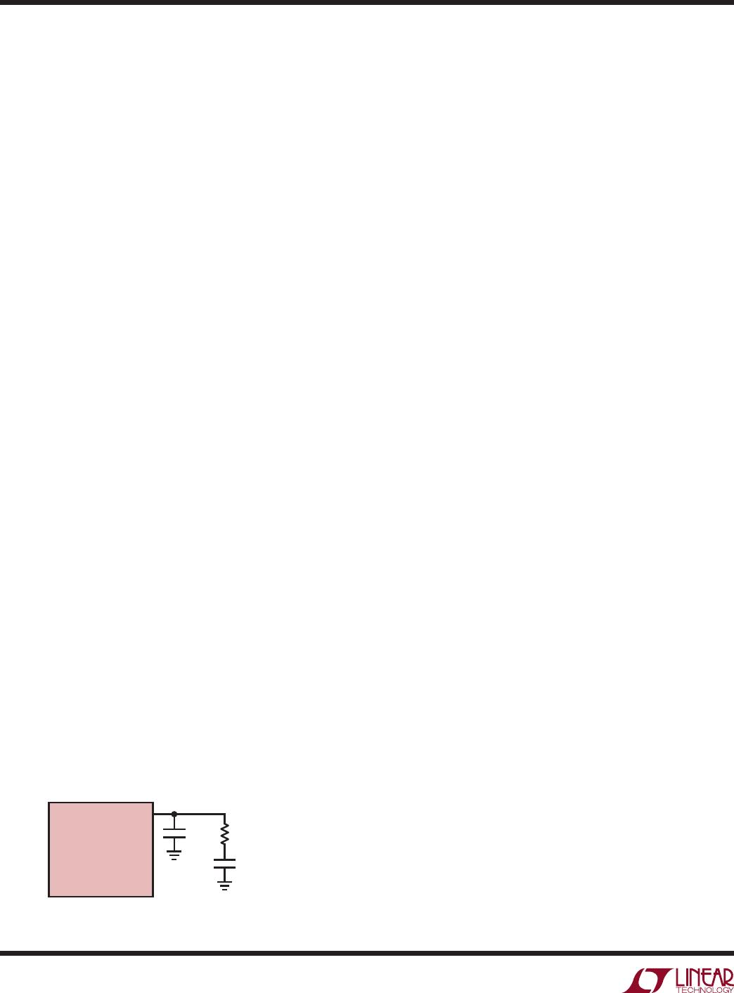
Parasitic MOSFET Oscillation
When the N-channel MOSFET ramps up the output dur
-
ing power-up it operates as a source follower. The source
follower configuration may self-oscillate in the range of
25
kHz to
300kHz when the load capacitance is less than
10µF, especially if the wiring inductance from the supply
to the V
DD
pin is greater than 3µH. The possibility of oscil-
lation will increase as the load current (during power-up)
increases.
There are two ways to prevent this type of
oscillation. The simplest way is to avoid load capacitances
below 10µF. For wiring inductance larger than 20µH, the
minimum load capacitance may extend to 100µF. A second
choice is to connect an external gate capacitor C
P
>1.5nF
as shown in Figure 3.
Turn-Off Sequence
The switch can be turned off by a variety of conditions. A
normal turn-off is initiated by either the EN1 or EN2 pins
going above their 1.235V threshold. Additionally, several
fault conditions will turn off the switch. These include over
-
current circuit breaker (SENSE pin) or overtemperature.
Normally the switch is turned off with a 250µ
A current
pulling down the GATE pin to ground. With the switch
turned off, the OUT voltage drops which pulls the FB pin
below its threshold. PG then goes high to indicate output
power is no longer good.
Figure 3. Compensation for Small C
LOAD
4219 F03
LTC4219
OPTIONAL
RC TO LOWER
INRUSH CURRENT
GATE
C
P
2.2nF

LTC4219IDHC-5#TRPBF

Mfr. #:
Manufacturer:
Analog Devices Inc.
Description:
Hot Swap Voltage Controllers 5V, 5A Integrated Hot Swap Controller
Lifecycle:
New from this manufacturer.
Delivery:
DHL FedEx Ups TNT EMS
Payment:
T/T Paypal Visa MoneyGram Western Union