LTC3026
1
3026ff
Typical applicaTion
FeaTures
applicaTions
DescripTion
1.5A Low Input Voltage
VLDO Linear Regulator
The LTC
®
3026 is a very low dropout (VLDO™) linear regula-
tor that can operate at input voltages down to 1.14V. The
device is capable of supplying 1.5A of output current with
a typical dropout voltage of only 100mV. To allow opera-
tion at low input voltages the LTC3026 includes a boost
converter that provides the necessary headroom for the
internal LDO circuitry.
Output current comes directly from the input supply to
maximize efficiency. The boost converter requires only a
small chip inductor and ceramic capacitor for operation.
Additionally, the boosted output voltage of one LTC3026
can supply the boost voltage for other LTC3026s, thus
requiring a single inductor for multiple LDOs. A user sup-
plied boost voltage can be used eliminating the need for
an inductor altogether.
The LTC3026 regulator is stable with 10µF or greater
ceramic output capacitors. The device has a low 0.4V
reference voltage which is used to program the output
voltage via two external resistors. The device also has
internal current limit, overtemperature shutdown, and
reverse output current protection. The LTC3026 is avail-
able in a small 10-lead MSOP or low profile (0.75mm)
10-lead 3mm × 3mm DFN package.
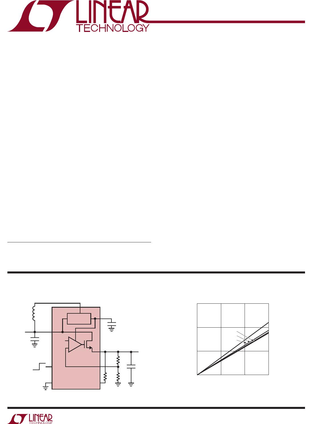
1.2V Output Voltage from 1.5V Input Supply
n
Input Voltage Range:
1.14V to 3.5V (with Boost Enabled)
1.14V to 5.5V (with External 5V Boost)
n
Low Dropout Voltage: 100mV at I
OUT
= 1.5A
n
Adjustable Output Range: 0.4V to 2.6V
n
Output Current: Up to 1.5A
n
Excellent Supply Rejection Even Near Dropout
n
Shutdown Disconnects Load from V
IN
and V
BST
n
Low Operating Current: I
IN
= 950µA at V
IN
= 1.5V
n
Low Shutdown Current:
I
IN
< 1µA (Typ), I
BST
= 0.1µA (Typ)
n
Stable with 10µF or Greater Ceramic Capacitors
n
Short-Circuit, Reverse Current Protected
n
Overtemperature Protected
n
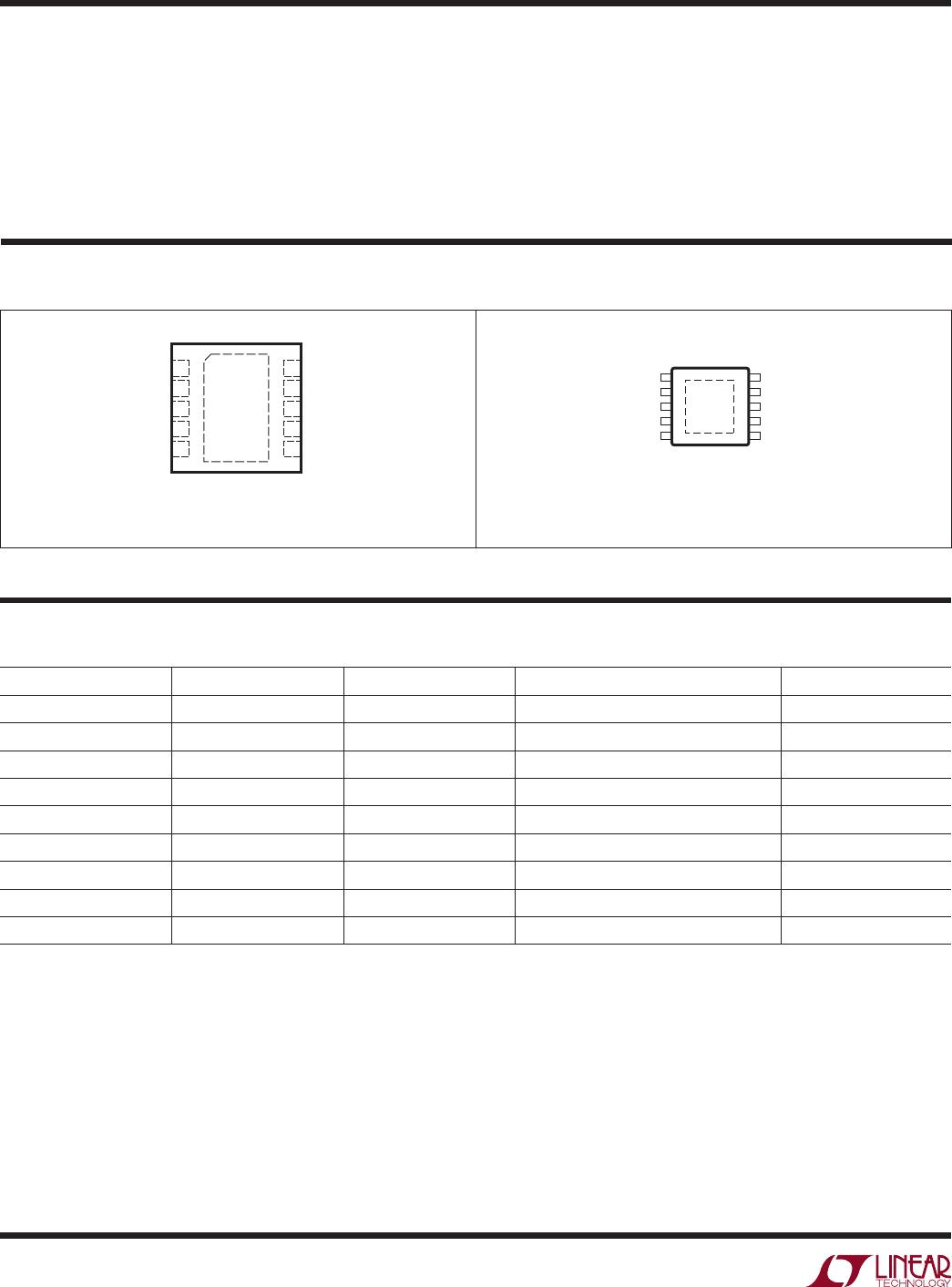
Available in 10-Lead MSOP and 10-Lead
(3mm × 3mm) DFN Packages
n
High Efficiency Linear Regulator
n
Post Regulator for Switching Supplies
n
Microprocessor Supply
Dropout Voltage vs Output Current
SW
IN
0.4V
OUT
BST
5V BOOST
CONVERTER
GND
ADJ
PG
L1
10µH
4.7µF
C
OUT
10µF
V
IN
= 1.5V
V
OUT
= 1.2V,
1.5A
OFF ON
100k
8.06k
4.02k
LTC3026
3026 TA01a
SHDN
L1: MURATA LQH2MCN100K02
+
4.7µF
I
OUT
(A)
0
DROPOUT (mV)
100
150
3026 TA01b
50
0
0.5
1.0
1.5
1.2V
1.5V
2.0V
2.6V
L, LT, LTC, LTM, Linear Technology, the Linear logo and Burst Mode are registered trademarks
and ThinSOT, VLDO are trademarks of Linear Technology Corporation. All other trademarks are
the property of their respective owners.
LTC3026
2
3026ff
absoluTe MaxiMuM raTings
V
BST
to GND ................................................. 0.3V to 6V
V
IN
to GND ................................................... 0.3V to 6V
PG to GND ................................................... 0.3V to 6V
SHDN to GND ............................................ 0.3V to 6.3V
ADJ to GND .................................. 0.3V to (V
IN
+ 0.3V)
(Note 1)
TOP VIEW
DD PACKAGE
10-LEAD (3mm
×
3mm) PLASTIC DFN
10
9
6
7
8
4
5
3
2
1
OUT
OUT
ADJ
PG
SHDN
IN
IN
GND
SW
BST
11
GND
T
JMAX
= 125°C, θ
JA
= 40°C/W
EXPOSED PAD (PIN 11) IS GND, MUST BE SOLDERED TO PCB
1
2
3
4
5
IN
IN
GND
SW
BST
10
9
8
7
6
OUT
OUT
ADJ
PG
SHDN
TOP VIEW
MSE PACKAGE
10-LEAD PLASTIC MSOP
11
GND
T
JMAX
= 125°C, θ
JA
= 40°C/W
EXPOSED PAD (PIN 11) IS GND, MUST BE SOLDERED TO PCB
pin conFiguraTion
orDer inForMaTion
LEAD FREE FINISH TAPE AND REEL PART MARKING PACKAGE DESCRIPTION TEMPERATURE RANGE
LTC3026EDD#PBF LTC3026EDD#TRPBF LBHW
10-Lead (3mm × 3mm) Plastic DFN
–40°C to 125°C
LTC3026IDD#PBF LTC3026IDD#TRPBF LBHW
10-Lead (3mm × 3mm) Plastic DFN
–40°C to 125°C
LTC3026EMSE#PBF LTC3026EMSE#TRPBF LTBJB 10-Lead Plastic MSOP –40°C to 125°C
LTC3026IMSE#PBF LTC3026IMSE#TRPBF LTBJB 10-Lead Plastic MSOP –40°C to 125°C
LEAD BASED FINISH TAPE AND REEL PART MARKING PACKAGE DESCRIPTION TEMPERATURE RANGE
LTC3026EDD LTC3026EDD#TR LBHW
10-Lead (3mm × 3mm) Plastic DFN
–40°C to 125°C
LTC3026IDD LTC3026IDD#TR LBHW
10-Lead (3mm × 3mm) Plastic DFN
–40°C to 125°C
LTC3026EMSE LTC3026EMSE#TR LTBJB 10-Lead Plastic MSOP –40°C to 125°C
LTC3026IMSE LTC3026IMSE#TR LTBJB 10-Lead Plastic MSOP –40°C to 125°C
Consult LTC Marketing for parts specified with wider operating temperature ranges.
For more information on lead free part marking, go to: http://www.linear.com/leadfree/
For more information on tape and reel specifications, go to: http://www.linear.com/tapeandreel/
Output Short-Circuit Duration .......................... Indefinite
Operating Junction Temperature Range
(Note 8) ............................................. 40°C to 125°C
Storage Temperature Range .................. 65°C to 125°C
Lead Temperature (MSE, Soldering, 10 sec) ......... 300°C
LTC3026
3
3026ff
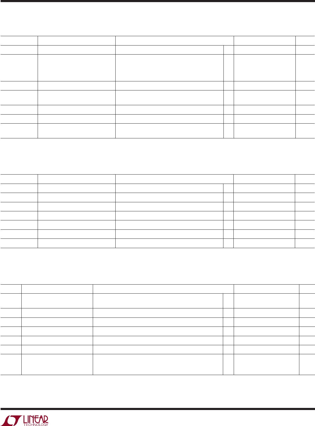
elecTrical characTerisTics
The l denotes the specifications which apply over the full operating junction temperature range, otherwise specifications are at
T
J
= 25°C. V
IN
= 1.5V, V
OUT
= 1.2V, C
IN
= C
BST
= 4.7µF, C
OUT
= 10µF (all capacitors ceramic) unless otherwise noted.
(BOOST ENABLED, L
SW
= 10µH)
SYMBOL PARAMETER CONDITIONS MIN TYP MAX UNITS
V
IN
Operating Voltage (Note 2)
l
1.14 5.5 V
I
IN
Operating Current I
OUT
= 100µA, V
SHDN
= V
IN
, 1.2V ≤ V
IN
≤ 5V
l
95 200 µA
I
INSHDN
Shutdown Current V
SHDN
= 0V, V
IN
= 3.5V
l
0.6 20 µA
V
BST
Boost Operating Voltage (Note 7) V
SHDN
= V
IN
l
4.5 5 5.5 V
V
BSTUVLO
Undervoltage Lockout
l
4.0 4.25 4.4 V
I
BST
Boost Operating Current I
OUT
= 100µA, V
SHDN
= V
IN
l
175 275 µA
I
BSTSHDN
Boost Shutdown Current V
SHDN
= 0V 1 5 µA
The l denotes the specifications which apply over the full operating junction temperature range, otherwise specifications are at
T
J
= 25°C. V
IN
= 1.5V, V
OUT
= 1.2V, V
BST
= 5V, C
IN
= C
BST
= 1µF, C
OUT
= 10µF (all capacitors ceramic) unless otherwise noted.
(BOOST DISABLED, V
SW
= 0V or Floating)
SYMBOL PARAMETER CONDITIONS MIN TYP MAX UNITS
V
ADJ
Regulation Voltage (Note 5) 1mA ≤ I
OUT
≤ 1.5A, 1.14V ≤ V
IN
≤ 3.5V, V
BST
= 5V, V
OUT
= 0.8V
1mA ≤ I
OUT
≤ 1.5A, 1.14V ≤ V
IN
≤ 3.5V, V
BST
= 5V, V
OUT
= 0.8V
l
0.397
0.395
0.4
0.4
0.403
0.405
V
V
OUT Programming Range
l
0.4 2.6 V
Dropout Voltage (Note 6) V
IN
= 1.5V, V
ADJ
= 0.38, I
OUT
= 1.5A
l
100 250 mV
I
ADJ
ADJ Input Current V
ADJ
= 0.4V
l
–100 100 nA
I
OUT
Continuous Output Current V
SHDN
= V
IN
l
1.5 A
I
LIM
Output Current Current Limit 3 A
e
n
Output Voltage Noise f = 10Hz to 100kHz, I
L
= 800mA
Boost Disabled
Boost Enabled
110
210
µV
RMS
µV
RMS
The l denotes the specifications which apply over the full operating junction temperature range, otherwise specifications are at
T
J
= 25°C. V
IN
= 1.5V, V
OUT
= 1.2V, C
IN
= C
BST
= 1µF, C
OUT
= 10µF (all capacitors ceramic) unless otherwise noted.
(BOOST ENABLED or DISABLED)
SYMBOL PARAMETER CONDITIONS MIN TYP MAX UNITS
V
IN
Operating Voltage (Note 2)
l
1.14 3.5 V
I
IN
Operating Current I
OUT
= 0mA, V
OUT
= 0.8V, V
SHDN
= V
IN
, V
IN
= 1.2V
I
OUT
= 0mA, V
OUT
= 1.2V, V
SHDN
= V
IN
, V
IN
= 1.5V
I
OUT
= 0mA, V
OUT
= 1.2V, V
SHDN
= V
IN
, V
IN
= 2.5V
I
OUT
= 0mA, V
OUT
= 1.2V, V
SHDN
= V
IN
, V
IN
= 3.5V
1160
950
640
400
µA
µA
µA
µA
I
INSHDN
Shutdown Current V
SHDN
= 0V, V
IN
= 3.5V
l
0.6 20 µA
Inductor Size Requirement
Inductor Peak Current Requirement
4.7
150
10 40 µH
mA
V
BST
Boost Output Voltage Range V
SHDN
= V
IN
4.8 5 5.2 V
V
BSTUVLO
Boost Undervoltage Lockout
l
4.0 4.2 4.4 V
Boost Output Drive (Note 3) V
IN
< 1.4V
V
IN
≥ 1.4V
7
10
mA
mA

LTC3026EMSE#PBF

Mfr. #:
Manufacturer:
Analog Devices / Linear Technology
Description:
LDO Voltage Regulators 1.5A VLDO in MSE
Lifecycle:
New from this manufacturer.
Delivery:
DHL FedEx Ups TNT EMS
Payment:
T/T Paypal Visa MoneyGram Western Union