LTC3026
13
3026ff
operaTion
temperatures, or in cases where internal power dissipa-
tion cause excessive self heating on-chip, the thermal
shutdown circuitry will shut down the boost converter and
LDO when the junction temperature exceeds approximately
150°C. It will reenable the converter and LDO once the
junction temperature drops back to approximately 140°C.
The LTC3026 will cycle in and out of thermal shutdown
without latchup or damage until the overstress condition
is removed. Long term overstress (T
J
> 125°C) should
be avoided as it can degrade the performance or shorten
the life of the part.
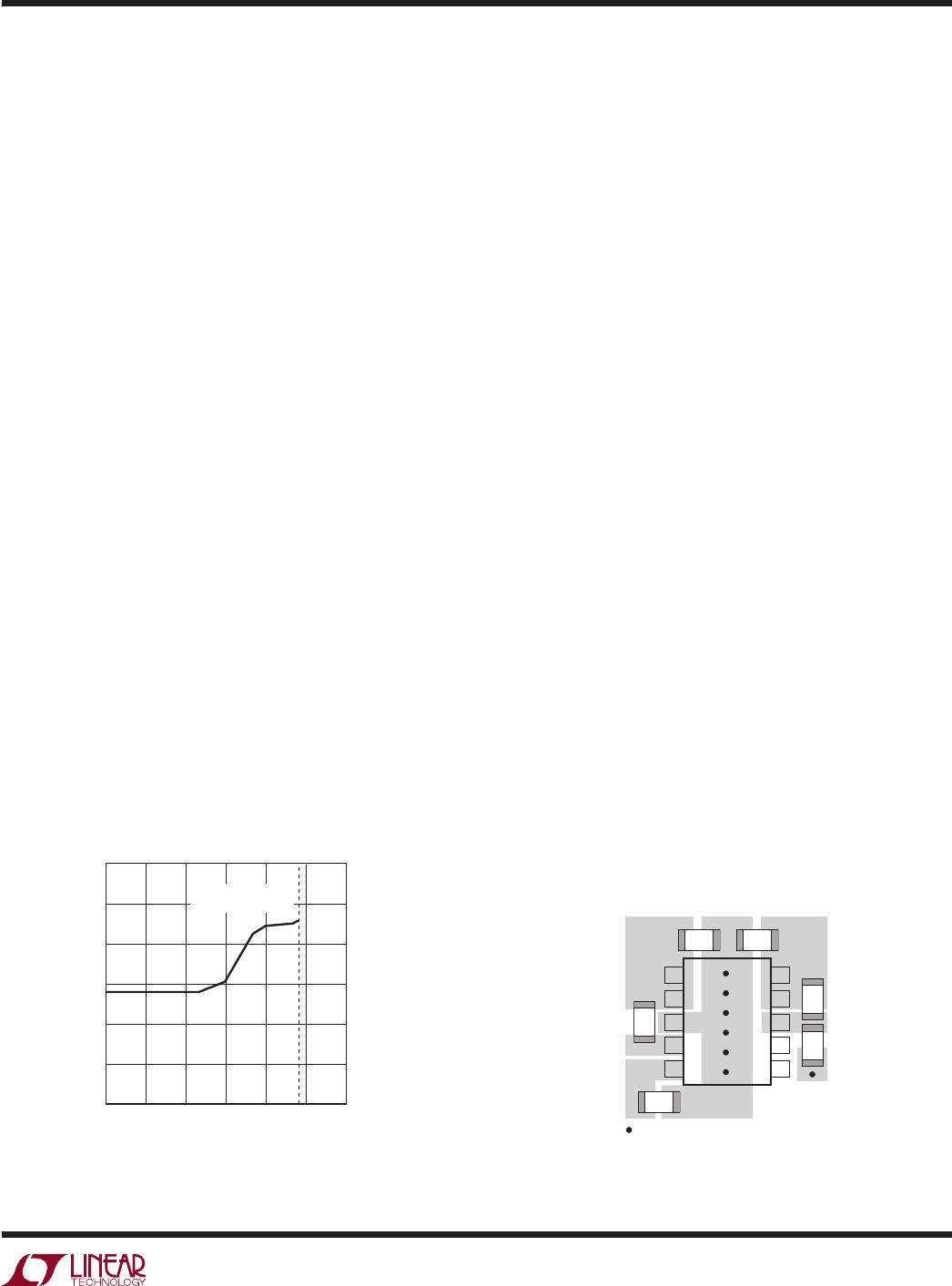
Reverse Input Current Protection
The LTC3026 features reverse input current protection to
limit current draw from any supplementary power source
at the output. Figure 6 shows the reverse output current
limit for constant input and output voltages cases. Note:
Positive input current represents current flowing into the
V
IN
pin of LTC3026.
With V
OUT
held at or below the output regulation voltage
and V
IN
varied, IN current flow will follow Figure 6’s curves.
I
IN
reverse current ramps up to about 16µA as the V
IN
approaches V
OUT
. Reverse input current will spike up as
V
IN
approaches within about 30mV of V
OUT
as the reverse
current protection circuitry is disabled and normal opera-
tion resumes. As V
IN
transitions above V
OUT
the reverse
current transitions into short-circuit current as long as
V
OUT
is held below the regulation voltage.
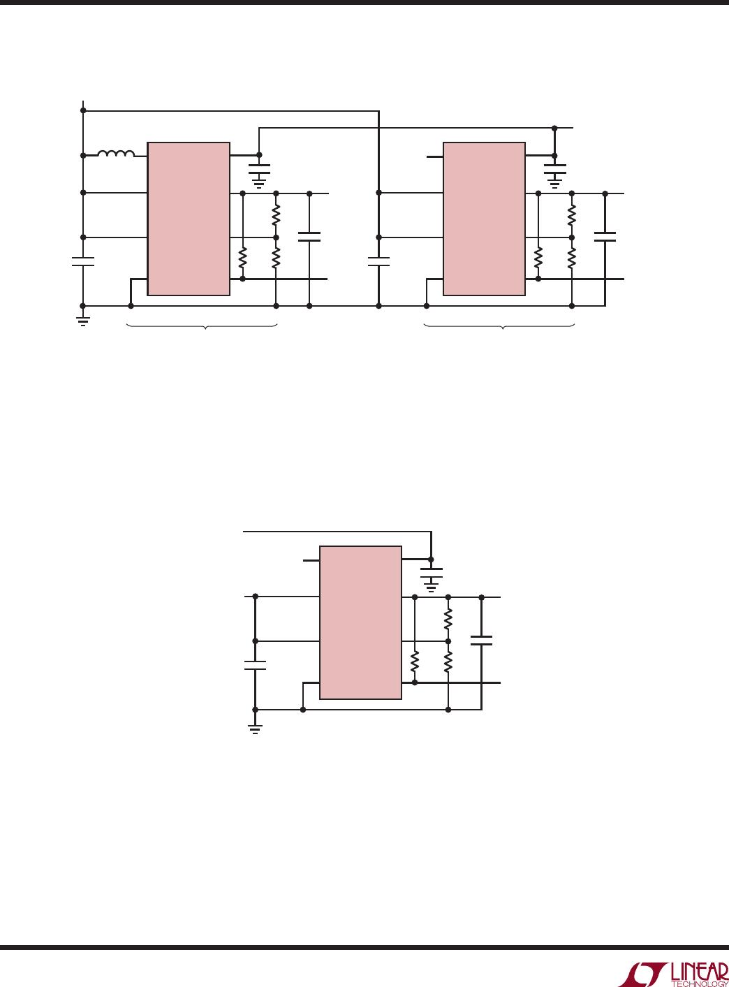
Layout Considerations
Connection from BST and OUT pins to their respec-
tive ceramic bypass capacitor should be kept as short
as possible. The ground side of the bypass capacitors
should be connected directly to the ground plane for best
results or through short traces back to the GND pin of the
part. Long traces will increase the effective series ESR
and inductance of the capacitor which can degrade
performance.
With the boost converter enabled, the SW pin will be
switching between ground and 5V whenever the BST pin
needs to be recharged. The transition edge rates of the SW
pin can be quite fast (~10ns). Thus care must be taken to
make sure the SW node does not couple capacitively to
other nodes (especially the ADJ pin). Additionally, stray
capacitance to this node reduces the efficiency and amount
of current available from the boost converter. For these
reasons it is recommended that the SW pin be connected
to the switching inductor with as short a trace as possible.
If the user has any sensitive nodes near the SW node, a
ground shield may be placed between the two nodes to
reduce coupling.
Because the ADJ pin is relatively high impedance (depend-
ing on the resistor divider used), stray capacitance at this
pin should be minimized (<10pF) to prevent phase shift
in the error amplifier loop. Additionally special attention
should be given to any stray capacitances that can couple
external signals onto the ADJ pin producing undesirable
output ripple. For optimum performance connect the ADJ
pin to R1 and R2 with a short PCB trace and minimize all
other stray capacitance to the ADJ pin.
Figure 6. Input Current vs Input Voltage
Figure 7. Suggested Layout
1
2
3
4
5
10
9
8
7
6
IN
IN
GND
SW
BST
OUT
OUT
ADJ
PG
SHDN
3026 F07
VIA CONNECTION TO GND PLANE
C
IN
C
OUT
L
SW
C
BST
R2
R1
INPUT VOLTAGE (V)
I
IN
CURRENT (µA)
3026 F06
30
20
10
0
–10
–20
–30
0
0.6
0.9
1.2
0.3
1.5
1.8
IN CURRENT
LIMIT ABOVE 1.45V