LTC3026
4
3026ff
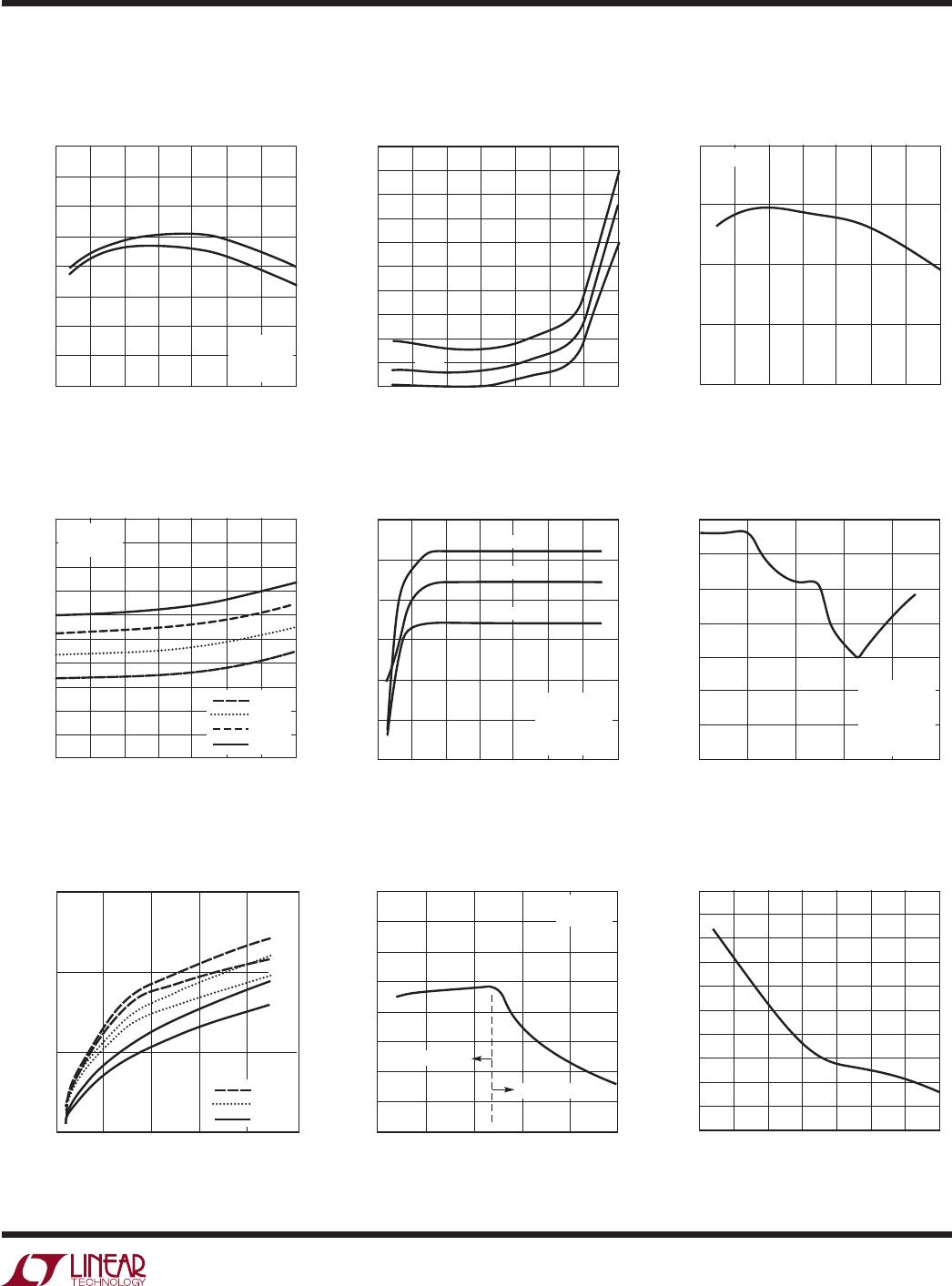
IN Supply Current with Boost
Converter Enabled
BST Supply Current with Boost
Converter Disabled
IN Supply Current with Boost
Converter Disabled
Typical perForMance characTerisTics
elecTrical characTerisTics
Note 1: Stresses beyond those listed under Absolute Maximum Ratings
may cause permanent damage to the device. Exposure to any Absolute
Maximum Rating condition for extended periods may affect device
reliability and lifetime. This IC has overtemperature protection that is
intended to protect the device during momentary overload conditions.
Junction temperatures will exceed 125°C when overtemperature is active.
Continuous operation above the specified maximum operating junction
temperature may impair device reliability.
Note 2: Minimum Operating Voltage required for regulation is:
V
IN
≥ V
OUT(MIN)
+ V
DROPOUT
Note 3: When using BST to drive loads other than LTC3026s, the load
must be high impedance during start-up (i.e. prior to PG going high).
Note 4: PG threshold expressed as a percentage difference from the
“V
ADJ
Regulation Voltage” as given in the table.
Note 5: Operating conditions are limited by maximum junction temperature.
The regulated output voltage specification will not apply for all possible
combinations of input voltage and output current. When operating at
maximum input voltage, the output current range must be limited. When
operating at maximum output current, the input voltage range must be limited.
Note 6: Dropout voltage is minimum input to output voltage differential
needed to maintain regulation at a specified output current. In dropout, the
output voltage will be equal to V
IN
– V
DROPOUT
.
Note 7: To maintain correct regulation
V
OUT
≤ V
BST
– 2.4V
Note 8: The LTC3026 is tested under pulsed load conditions such
that T
J
≈ T
A
. The LTC3026E is guaranteed to meet specifications from
0°C to 125°C junction temperature. Specifications over the –40°C to
125°C operating junction temperature range are assured by design,
characterization and correlation with statistical process controls. The
LTC3026I is guaranteed over the –40°C to 125°C operating junction
temperature range. Note that the maximum ambient temperature
consistent with these specifications is determined by specific operating
conditions in conjunction with board layout, the rated package thermal
impedance and other environmental factors. The junction temperature
(T
J
, in °C) is calculated from the ambient temperature (T
A
, in °C) and
power dissipation (P
D
, in watts) according to the formula:
T
J
= T
A
+ (P
D
• θ
JA
), where θ
JA
(in °C/W) is the package thermal
impedance.
3026 G01
V
IN
(V)
1.0
INPUT CURRENT (mA)
1.50
1.25
1.00
0.75
0.50
0.25
0
1.5 2.0 2.5 3.0
3.5
–40°C
25°C
85°C
3026 G02
V
IN
(V)
1.0
I
BST
(µA)
5.54.0 4.5 5.0
1.5
2.0 2.5
3.53.0
200
150
100
50
0
–40°C
25°C
85°C
125°C
V
BST
= 5V
3026 G03
V
IN
(V)
1.0 5.54.0 4.5 5.0
1.5
2.0 2.5
3.53.0
I
IN
(µA)
200
150
100
50
0
–40°C
25°C
85°C
125°C
V
BST
= 5V
The l denotes the specifications which apply over the full operating junction temperature range, otherwise specifications are at
T
J
= 25°C. V
IN
= 1.5V, V
OUT
= 1.2V, C
IN
= C
BST
= 1µF, C
OUT
= 10µF (all capacitors ceramic) unless otherwise noted.
(BOOST ENABLED or DISABLED)
SYMBOL PARAMETER CONDITIONS MIN TYP MAX UNITS
V
IHSHDN
SHDN Input High Voltage 1.14V ≤ V
IN
≤ 3.5V
3.5V ≤ V
IN
≤ 5.5V
l
l
1.0
1.2
V
V
V
ILSHDN
SHDN Input Low Voltage 1.14V ≤ V
IN
≤ 5.5V
l
0.4 V
I
IHSHDN
SHDN Input High Current SHDN = V
IN
–1 1 µA
I
ILSHDN
SHDN Input Low Current SHDN = 0V –1 1 µA
V
OLPG
PG Output Low Voltage I
PG
= 2mA
l
0.1 0.4 V
I
OHPG
PG Output High Leakage Current V
PG
= 5.5V 0.01 1 µA
PG Output Threshold (Note 4) PG High to Low
PG Low to High
–12
–10
–9
–7
–6
–4
%
%