General Description
High-speed DDR4 SDRAM modules use DDR4 SDRAM devices with two or four internal
memory bank groups. DDR4 SDRAM modules utilizing 4- and 8-bit-wide DDR4 SDRAM
devices have four internal bank groups consisting of four memory banks each, provid-
ing a total of 16 banks. 16-bit-wide DDR4 SDRAM devices have two internal bank
groups consisting of four memory banks each, providing a total of eight banks. DDR4
SDRAM modules benefit from DDR4 SDRAM's use of an 8n-prefetch architecture with
an interface designed to transfer two data words per clock cycle at the I/O pins. A single
READ or WRITE operation for the DDR4 SDRAM effectively consists of a single 8n-bit-
wide, four-clock data transfer at the internal DRAM core and eight corresponding n-bit-
wide, one-half-clock-cycle data transfers at the I/O pins.
DDR4 modules use two sets of differential signals: DQS_t and DQS_c to capture data
and CK_t and CK_c to capture commands, addresses, and control signals. Differential
clocks and data strobes ensure exceptional noise immunity for these signals and pro-
vide precise crossing points to capture input signals.
Fly-By Topology
DDR4 modules use faster clock speeds than earlier DDR technologies, making signal
quality more important than ever. For improved signal quality, the clock, control, com-
mand, and address buses have been routed in a fly-by topology, where each clock, con-
trol, command, and address pin on each DRAM is connected to a single trace and ter-
minated (rather than a tree structure, where the termination is off the module near the
connector). Inherent to fly-by topology, the timing skew between the clock and DQS sig-
nals can be easily accounted for by using the write-leveling feature of DDR4.
Module Manufacturing Location
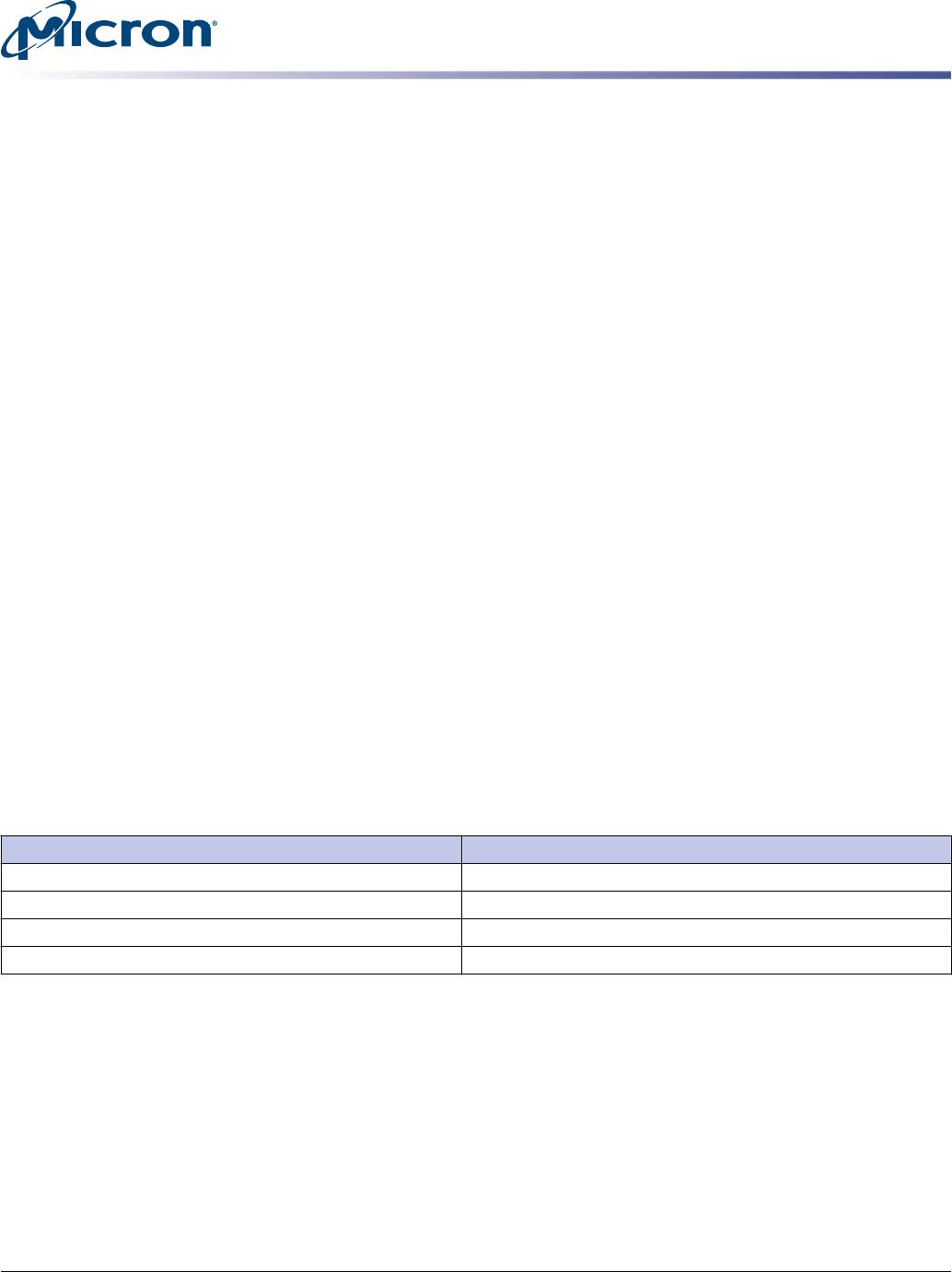
Micron Technology manufactures modules at sites world-wide. Customers may receive
modules from any of the following manufacturing locations:
Table 7: DRAM Module Manufacturing Locations
Manufacturing Site Location Country of Origin Specified on Label
Boise, USA USA
Aguadilla, Puerto Rico Puerto Rico
Xian, China China
Singapore Singapore
8GB (x64, SR) 260-Pin DDR4 SODIMM
General Description
CCMTD-1725822587-9885
atf8c1gx64hz.pdf – Rev. F 9/16 EN
10
Micron Technology, Inc. reserves the right to change products or specifications without notice.
© 2015 Micron Technology, Inc. All rights reserved.
Address Mapping to DRAM
Address Mirroring
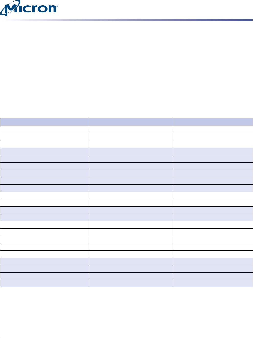
To achieve optimum routing of the address bus on DDR4 multi rank modules, the ad-
dress bus will be wired as shown in the table below, or mirrored. For quad rank mod-
ules, ranks 1 and 3 are mirrored and ranks 0 and 2 are non-mirrored. Highlighted ad-
dress pins have no secondary functions allowing for normal operation when cross-
wired. Data is still read from the same address it was written. However, Load Mode op-
erations require a specific address. This requires the controller to accommodate for a
rank that is "mirrored." Systems may reference DDR4 SPD to determine if the module
has mirroring implemented or not. See the JEDEC DDR4 SPD specification for more de-
tails.
Table 8: Address Mirroring
Edge Connector Pin DRAM Pin, Non-mirrored DRAM Pin, Mirrored
A0 A0 A0
A1 A1 A1
A2 A2 A2
A3 A3 A4
A4 A4 A3
A5 A5 A6
A6 A6 A5
A7 A7 A8
A8 A8 A7
A9 A9 A9
A10 A10 A10
A11 A11 A13
A13 A13 A11
A12 A12 A12
A14 A14 A14
A15 A15 A15
A16 A16 A16
A17 A17 A17
BA0 BA0 BA1
BA1 BA1 BA0
BG0 BG0 BG1
BG1 BG1 BG0
8GB (x64, SR) 260-Pin DDR4 SODIMM
Address Mapping to DRAM
CCMTD-1725822587-9885
atf8c1gx64hz.pdf – Rev. F 9/16 EN
11
Micron Technology, Inc. reserves the right to change products or specifications without notice.
© 2015 Micron Technology, Inc. All rights reserved.
SPD EEPROM Operation
DDR4 SDRAM modules incorporate serial presence detect (SPD). The SPD data is stor-
ed in a 512-byte JEDEC JC-42.4-compliant EEPROM that is segregated into four 128-
byte, write-protectable blocks. The SPD content is aligned with these blocks as shown in
the table below.
Block Range Description
0 0–127 000h–07Fh Configuration and DRAM parameters
1 128–255 080h–0FFh Module-specific parameters
2 256–319 100h–13Fh Reserved; all bytes coded as 00h
320–383 140h–17Fh Manufacturing information
3 384–511 180h–1FFh End-user programmable
The first 384 bytes are programmed by Micron to comply with JEDEC standard JC-45,
"Appendix X: Serial Presence Detect (SPD) for DDR4 SDRAM Modules." The remaining
128 bytes of storage are available for use by the customer.
The EEPROM resides on a two-wire I
2
C serial interface and is not integrated with the
memory bus in any way. It operates as a slave device in the I
2
C bus protocol, with all
operations synchronized by the serial clock. Transfer rates of up to 1 MHz are achieva-
ble at 2.5V (NOM).
Micron implements reversible software write protection on DDR4 SDRAM-based mod-
ules. This prevents the lower 384 bytes (bytes 0–383) from being inadvertently program-
med or corrupted. The upper 128 bytes remain available for customer use and unpro-
tected.
8GB (x64, SR) 260-Pin DDR4 SODIMM
SPD EEPROM Operation
CCMTD-1725822587-9885
atf8c1gx64hz.pdf – Rev. F 9/16 EN
12
Micron Technology, Inc. reserves the right to change products or specifications without notice.
© 2015 Micron Technology, Inc. All rights reserved.

MTA8ATF1G64HZ-2G3B1

Mfr. #:
Manufacturer:
Micron
Description:
IC SDRAM DDR4 8GB 1GX64 FBGA
Lifecycle:
New from this manufacturer.
Delivery:
DHL FedEx Ups TNT EMS
Payment:
T/T Paypal Visa MoneyGram Western Union