LTC3411
16
3411fb
To avoid the LTC3411 from exceeding the maximum junc-
tion temperature, the user will need to do some thermal
analysis. The goal of the thermal analysis is to determine
whether the power dissipated exceeds the maximum
junction temperature of the part. The temperature rise is
given by:
T
RISE
= P
D
• θ
JA
where P
D
is the power dissipated by the regulator and θ
JA
is the thermal resistance from the junction of the die to
the ambient temperature.
The junction temperature, T
J
, is given by:
T
J
= T
RISE
+ T
AMBIENT
As an example, consider the case when the LTC3411 is
in dropout at an input voltage of 3.3V with a load current
of 1A. From the Typical Performance Characteristics
graph of Switch Resistance, the R
DS(ON)
resistance of the
P-channel switch is 0.11Ω. Therefore, power dissipated
by the part is:
P
D
= I
2
• R
DS(ON)
= 110mW
The MS10 package junction-to-ambient thermal resistance,
θ
JA
, will be in the range of 100°C/W to 120°C/W. Therefore,
the junction temperature of the regulator operating in a
70°C ambient temperature is approximately:
T
J
= 0.11 • 120 + 70 = 83.2°C
Remembering that the above junction temperature is
obtained from an R
DS(ON)
at 25°C, we might recalculate
the junction temperature based on a higher R
DS(ON)
since
it increases with temperature. However, we can safely as-
sume that the actual junction temperature will not exceed
the absolute maximum junction temperature of 125°C.
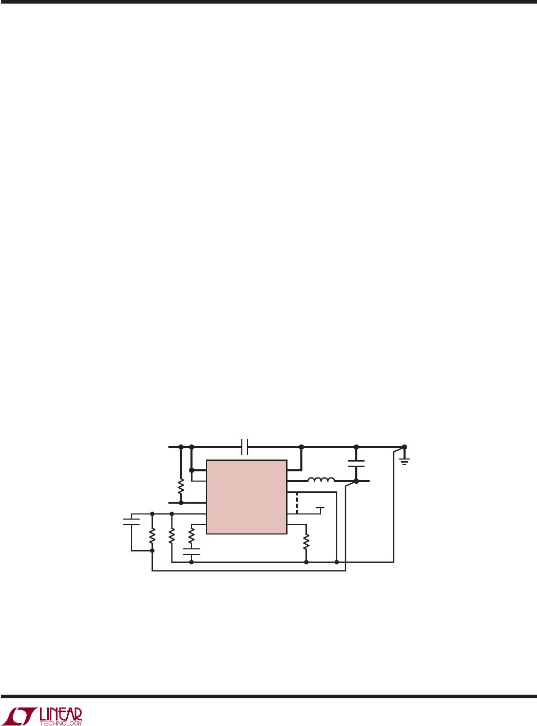
APPLICATIONS INFORMATION
Design Example
As a design example, consider using the LTC3411 in a por-
table application with a Li-Ion battery. The battery provides
a V
IN
= 2.5V to 4.2V. The load requires a maximum of 1A
in active mode and 10mA in standby mode. The output
voltage is V
OUT
= 2.5V. Since the load still needs power in
standby, Burst Mode operation is selected for good low
load effi ciency.
First, calculate the timing resistor:
R MHz k
T
=
()
=
−
9 78 10 1 323 8
11
108
.• .
.
Use a standard value of 324k. Next, calculate the inductor
value with 40% ripple current which is 500mA
:
L
V
MHz mA
V
V
H=−
⎛
⎝
⎜
⎞
⎠
⎟
=μ
25
1 500
1
25
42
2
.
•
•
.
.
Choosing the closest inductor from a vendor of 2.2μH,
results in a maximum ripple current of:
Δ=
μ
−
⎛
⎝
⎜
⎞
⎠
⎟
=I
V
MHz
V
V
mA
L
25
122
1
25
42
460
.
•.
•
.
.
For cost reasons, a ceramic capacitor will be used. C
OUT
selection is then based on load step droop instead of ESR
requirements. For a 5% output droop:
C
A
MHz V
F
OUT
≈=μ25
1
1525
20.
•( %• . )
The closest standard value is 22μF. Since the output
impedance of a Li-Ion battery is very low, C
IN
is typically
10μF. In noisy environments, decoupling SV
IN
from PV
IN
with an R6/C8 fi lter of 1Ω/0.1μF may help, but is typically
not needed.