LTC3411
8
3411fb
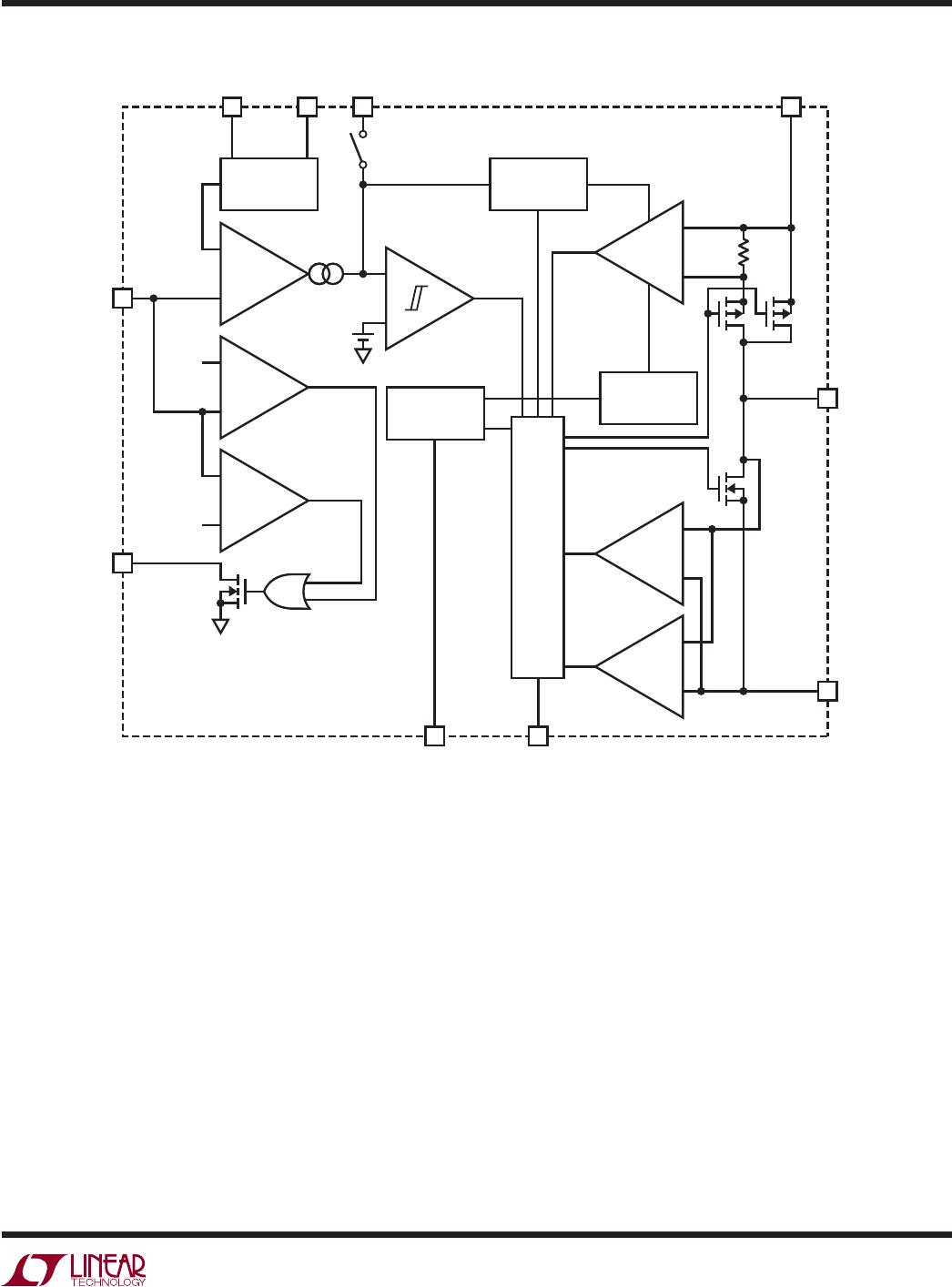
OPERATION
The LTC3411 uses a constant frequency, current mode
architecture. The operating frequency is determined by
the value of the R
T
resistor or can be synchronized to an
external oscillator. To suit a variety of applications, the
selectable Mode pin, allows the user to trade-off noise
for effi ciency.
The output voltage is set by an external divider returned
to the V
FB
pin. An error amplfi er compares the divided
output voltage with a reference voltage of 0.8V and adjusts
the peak inductor current accordingly. Overvoltage and
undervoltage comparators will pull the PGOOD output
low if the output voltage is not within ±7.5%.
Main Control Loop
During normal operation, the top power switch (P-channel
MOSFET) is turned on at the beginning of a clock cycle when
the V
FB
voltage is below the reference voltage. The current
into the inductor and the load increases until the current
limit is reached. The switch turns off and energy stored in
the inductor fl ows through the bottom switch (N-channel
MOSFET) into the load until the next clock cycle.
The peak inductor current is controlled by the voltage
on the I
TH
pin, which is the output of the error amplifi er.
This amplifi er compares the V
FB
pin to the 0.8V reference.
When the load current increases, the V
FB
voltage decreases
slightly below the reference. This decrease causes the
error amplifi er to increase the I
TH
voltage until the average
inductor current matches the new load current.
The main control loop is shut down by pulling the SHDN/R
T
pin to SV
IN
. A digital soft-start is enabled after shutdown,
which will slowly ramp the peak inductor current up over
1024 clock cycles or until the output reaches regulation,
whichever is fi rst. Soft-start can be lengthened by ramping
the voltage on the I
TH
pin (see Applications Information
section).
Low Current Operation
Three modes are available to control the operation of the
LTC3411 at low currents. All three modes automatically
switch from continuous operation to the selected mode
when the load current is low.
To optimize effi ciency, the Burst Mode operation can be
selected. When the load is relatively light, the LTC3411
automatically switches into Burst Mode operation in which
the PMOS switch operates intermittently based on load
demand. By running cycles periodically, the switching
losses which are dominated by the gate charge losses of
the power MOSFETs are minimized. The main control loop
is interrupted when the output voltage reaches the desired
regulated value. The hysteretic voltage comparator B
trips when I
TH
is below 0.24V, shutting off the switch and
reducing the power. The output capacitor and the inductor
supply the power to the load until I
TH
/RUN exceeds 0.31V,
turning on the switch and the main control loop which
starts another cycle.
For lower output voltage ripple at low currents, pulse
skipping mode can be used. In this mode, the LTC3411
continues to switch at a constant frequency down to
very low currents, where it will eventually begin skipping
pulses.
Finally, in forced continuous mode, the inductor current
is constantly cycled which creates a fi xed output voltage
ripple at all output current levels. This feature is desirable
in telecommunications since the noise is at a constant
frequency and is thus easy to fi lter out. Another advan-
tage of this mode is that the regulator is capable of both
sourcing current into a load and sinking some current
from the output.
Dropout Operation
When the input supply voltage decreases toward the
output voltage, the duty cycle increases to 100% which
is the dropout condition. In dropout, the PMOS switch is
turned on continuously with the output voltage being equal
to the input voltage minus the voltage drops across the
internal P-channel MOSFET and the inductor.
Low Supply Operation
The LTC3411 incorporates an undervoltage lockout circuit
which shuts down the part when the input voltage drops
below about 2.5V to prevent unstable operation.