LTC3388-1/LTC3388-3
1
338813fa
For more information www.linear.com/LTC3388
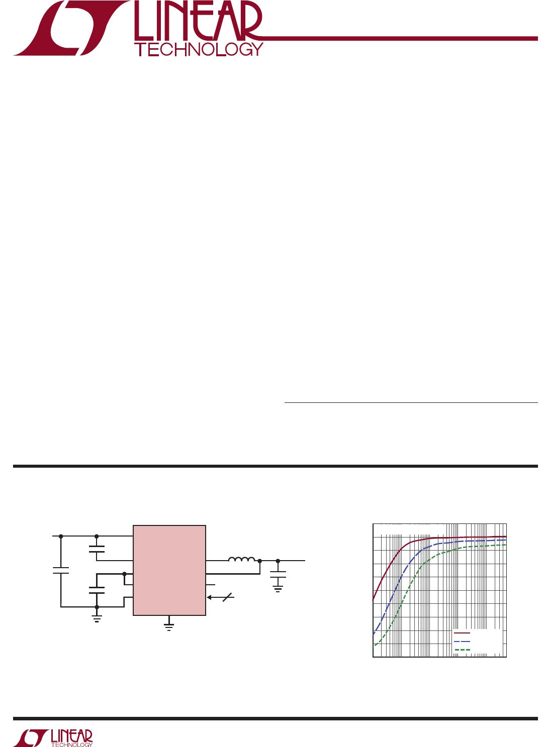
TYPICAL APPLICATION
FEATURES DESCRIPTION
20V High Efficiency
Nanopower
Step-Down Regulator
The LTC
®
3388-1/LTC3388-3 are high efficiency step-down
DC/DC converters with internal high side and synchronous
power switches that draw only 720nA typical DC supplycur-
rent at no load while maintaining output voltage regulation.
Capable of supplying 50mA of load current, the LTC3388-1/
LTC3388-3 also incorporate an accurate undervoltage
lockout (UVLO) feature to disable the converter and main-
tain a low quiescent current state when the input voltage
falls below 2.3V. In regulation, the LTC3388-1/LTC3388-3
enter a sleep state in which both input and output quies-
cent currents are minimal. The buck converter turns on
and off as needed to maintain regulation. An additional
standby mode disables buck switching while the output is
in regulation for short duration loads requiring low ripple.
Output voltages of 1.2V, 1.5V, 1.8V, 2.5V (LTC3388-1)
and 2.8V, 3.0V, 3.3V, 5.0V (LTC3388-3) are pin selectable.
The LTC3388-1/LTC3388-3 can operate with V
IN
up to 20V
while the no load quiescent current remains below 1µA.
L, LT , LT C , LT M, Linear Technology, the Linear logo and Burst Mode are registered trademarks
of Linear Technology Corporation. All other trademarks are the property of their respective
owners.
50mA Step-Down Converter
APPLICATIONS
n
720nA Input I
Q
in Regulation (No Load), V
IN
= 4V
n
820nA Input I
Q
in Regulation (No Load), V
IN
= 20V
n
400nA Input I
Q
in UVLO
n
2.7V to 20V Input Operating Range
n
Up to 50mA of Output Current
n
Pin Selectable Output Voltages:
n
1.2V, 1.5V, 1.8V, 2.5V (LTC3388-1)
n
2.8V, 3.0V, 3.3V, 5.0V (LTC3388-3)
n
High Efficiency Hysteretic Synchronous
DC/DC Conversion
n
Standby Mode Disables Buck Switching
n
Available in 10-Lead MSE and 3mm × 3mm
DFN Packages
n
Keep Alive Power for Portable Products
n
Industrial Control Supplies
n
Distributed Power Systems
n
Battery-Operated Devices
338813 TA01a
V
IN
CAP
V
IN2
EN
STBY
SW
V
OUT
PGOOD
D0, D1
LTC3388-1/
LTC3388-3
GND
1µF
6V
4.7µF
6V
2.2µF
25V
2.7V TO 20V
47µF
6V
OUTPUT
VOLTAGE
SELECT
V
OUT
100µH
2
Efficiency vs Load Current
LOAD CURRENT (A)
EFFICIENCY (%)
100
40
50
30
20
80
90
70
60
10
0
100µ 1m 10m1µ 10µ
V
OUT
= 1.8V, L = 100µH
V
IN
= 3.0V
V
IN
= 10V
V
IN
= 20V