LTC3388-1/LTC3388-3
7
338813fa
For more information www.linear.com/LTC3388
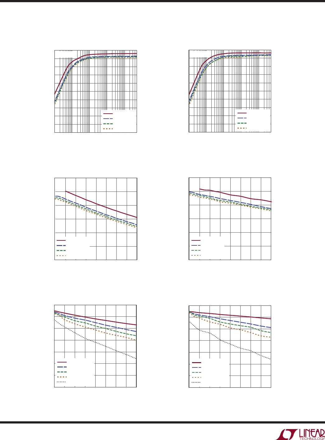
TYPICAL PERFORMANCE CHARACTERISTICS
Efficiency vs I
LOAD
, L = 22µH
(LTC3388-1)
Efficiency vs V
IN
for I
LOAD
= 50mA,
L = 22µH (LTC3388-1)
Efficiency vs V
IN
for V
OUT
= 1.8V,
L = 22µH (LTC3388-1)
Efficiency vs I
LOAD
, L = 100µH
(LTC3388-1)
Efficiency vs V
IN
for I
LOAD
= 50mA,
L = 100µH (LTC3388-1)
Efficiency vs V
IN
for V
OUT
= 1.8V,
L = 100µH (LTC3388-1)
LOAD CURRENT (A)
EFFICIENCY (%)
100
40
50
60
70
80
90
30
20
10
0
338813 G22
10m 1m100µ10µ
V
OUT
= 2.5V
V
OUT
= 1.8V
V
OUT
= 1.5V
V
OUT
= 1.2V
V
IN
= 3.0V
LOAD CURRENT (A)
EFFICIENCY (%)
100
40
50
60
70
80
90
30
20
10
0
338813 G23
10m 1m100µ10µ
V
IN
= 3.0V
V
OUT
= 2.5V
V
OUT
= 1.8V
V
OUT
= 1.5V
V
OUT
= 1.2V
V
IN
(V)
EFFICIENCY (%)
100
90
95
80
85
75
70
338813 G24
12 14 16 18 202 4 1086
V
OUT
= 2.5V
V
OUT
= 1.8V
V
OUT
= 1.5V
V
OUT
= 1.2V
V
IN
(V)
EFFICIENCY (%)
100
90
95
80
85
75
70
338813 G25
12 14 16 18 202 4 1086
V
OUT
= 2.5V
V
OUT
= 1.8V
V
OUT
= 1.5V
V
OUT
= 1.2V
V
IN
(V)
EFFICIENCY (%)
100
70
80
90
50
60
40
30
338813 G26
12 14 16 18 202 4 1086
I
LOAD
= 50mA
I
LOAD
= 100µA
I
LOAD
= 50µA
I
LOAD
= 30µA
I
LOAD
= 10µA
V
IN
(V)
EFFICIENCY (%)
100
70
80
90
50
60
40
30
338813 G27
12 14 16 18 202 4 1086
I
LOAD
= 50mA
I
LOAD
= 100µA
I
LOAD
= 50µA
I
LOAD
= 30µA
I
LOAD
= 10µA
LTC3388-1/LTC3388-3
8
338813fa
For more information www.linear.com/LTC3388
TYPICAL PERFORMANCE CHARACTERISTICS
Efficiency vs I
LOAD
, L = 100µH
(LTC3388-3)
Efficiency vs V
IN
for I
LOAD
= 50mA,
L = 100µH (LTC3388-3)
Efficiency vs V
IN
for V
OUT
= 3.3V,
L = 100µH (LTC3388-3)
Efficiency vs I
LOAD
, L = 22µH
(LTC3388-3)
Efficiency vs V
IN
for I
LOAD
= 50mA,
L = 22µH (LTC3388-3)
Efficiency vs V
IN
for V
OUT
= 3.3V,
L = 22µH (LTC3388-3)
LOAD CURRENT (A)
EFFICIENCY (%)
100
50
60
90
70
20
10
30
40
80
0
338813 G28
10m100µ 1m10µ
V
OUT
= 5.0V
V
OUT
= 3.3V
V
OUT
= 3.0V
V
OUT
= 2.8V
V
IN
= 6.0V
LOAD CURRENT (A)
EFFICIENCY (%)
100
50
60
90
70
20
10
30
40
80
0
338813 G29
10m100µ 1m10µ
V
IN
= 6.0V
V
OUT
= 5.0V
V
OUT
= 3.3V
V
OUT
= 3.0V
V
OUT
= 2.8V
V
IN
(V)
EFFICIENCY (%)
100
80
85
90
95
75
70
338813 G30
141210 16 18 204 86
V
OUT
= 5.0V
V
OUT
= 3.3V
V
OUT
= 3.0V
V
OUT
= 2.8V
V
IN
(V)
EFFICIENCY (%)
100
80
85
90
95
75
70
338813 G31
141210 16 18 204 86
V
OUT
= 5.0V
V
OUT
= 3.3V
V
OUT
= 3.0V
V
OUT
= 2.8V
V
IN
(V)
EFFICIENCY (%)
100
70
80
90
50
60
40
30
338813 G32
12 14 16 18 204 1086
I
LOAD
= 50mA
I
LOAD
= 100µA
I
LOAD
= 50µA
I
LOAD
= 30µA
I
LOAD
= 10µA
V
IN
(V)
EFFICIENCY (%)
100
70
80
90
50
60
40
30
338813 G33
12 14 16 18 204 1086
I
LOAD
= 50mA
I
LOAD
= 100µA
I
LOAD
= 50µA
I
LOAD
= 30µA
I
LOAD
= 10µA
LTC3388-1/LTC3388-3
9
338813fa
For more information www.linear.com/LTC3388
PIN FUNCTIONS
EN (Pin 1): Enable Input. Logic level input referenced to
V
IN2
. A logic high on EN will enable the buck converter.
Driving EN to V
IN2
will result in no additional quiescent
current on V
IN
. However, if EN is driven near V
IH
or V
IL
40nA of additional quiescent current can appear on V
IN
.
STBY (Pin 2): Standby Input. Logic level input referenced
to V
IN2
. A logic high on STBY will place the part in standby
mode. Driving STBY to V
IN2
will result in no additional
quiescent current on V
IN
. However, if STBY is driven
near V
IH
or V
IL
40nA of additional quiescent current can
appear on V
IN
.
CAP (Pin 3): Internal rail referenced to V
IN
to serve as gate
drive for buck PMOS switch. A F capacitor should be
connected between CAP and V
IN
. This pin is not intended
for use as an external system rail.
V
IN
(Pin 4): Input Voltage. A 2.2µF or larger capacitor
should be connected from V
IN
to GND.
SW (Pin 5): Switch Pin for the Buck Switching Regulator.
A 22µH or larger inductor should be connected from SW
to V
OUT
.
V
OUT
(Pin 6): Sense pin used to monitor the output volt-
age and adjust it through internal feedback.
V
IN2
(Pin 7): Internal low voltage rail to serve as gate drive
for buck NMOS switch. Also serves as a logic high rail for
output voltage select bits D0 and D1. A 4.7µF capacitor
should be connected from V
IN2
to GND. This pin is not
intended for use as an external system rail.
D1 (Pin 8): Output Voltage Select Bit. D1 should be tied
high to V
IN2
or low to GND to select desired V
OUT
(see
Table 1).
D0 (Pin 9): Output Voltage Select Bit. D0 should be tied
high to V
IN2
or low to GND to select desired V
OUT
(see
Table 1).
PGOOD (Pin 10): Power Good Open-Drain NMOS Output.
The PGOOD pin is Hi-Z when V
OUT
is above 92% of the
target value.
GND (Exposed Pad Pin 11): Ground. The exposed pad
should be connected to a continuous ground plane on the
second layer of the printed circuit board by several vias
directly under the LTC3388-1/LTC3388-3.

LTC3388EDD-1#PBF

Mfr. #:
Manufacturer:
Analog Devices / Linear Technology
Description:
Switching Voltage Regulators 20V/50mA High Efficiency Step-Down Regulator with <1uA Quiescent Current
Lifecycle:
New from this manufacturer.
Delivery:
DHL FedEx Ups TNT EMS
Payment:
T/T Paypal Visa MoneyGram Western Union