LTC3388-1/LTC3388-3
11
338813fa
For more information www.linear.com/LTC3388
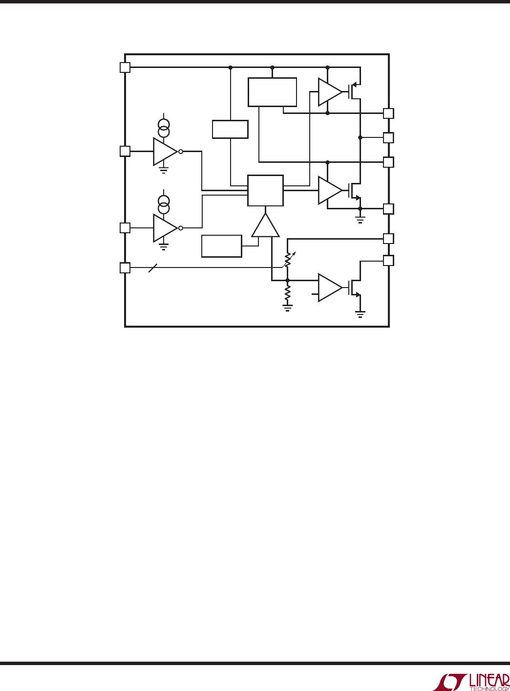
OPERATION
The LTC3388-1/LTC3388-3 is an ultralow quiescent
current power supply designed to maintain a regulated
output voltage by means of a nanopower high efficiency
synchronous buck regulator.
Undervoltage Lockout (UVLO)
When the voltage on V
IN
rises above the UVLO rising
threshold the buck converter is enabled and charge is
transferred from the input capacitor to the output ca-
pacitor. If V
IN
falls below the UVLO falling threshold the
part will re-enter UVLO. In UVLO the quiescent current is
approximately 400nA and the buck converter is disabled.
Internal Rail Generation
Two internal rails, CAP and V
IN2
, are generated from V
IN
and are used to drive the high side PMOS and low side
NMOS of the buck converter, respectively. Additionally the
V
IN2
rail serves as logic high for EN, STBY, and output
voltage select bits D0 and D1. The V
IN2
rail is regulated
at 4.6V above GND while the CAP rail is regulated at 4.8V
below V
IN
. The V
IN2
and CAP rails are not intended to be
used as external rails. Bypass capacitors are connected
to the CAP and V
IN2
pins to serve as energy reservoirs for
driving the buck switches. When V
IN
is below 4.6V, V
IN2
is equal to V
IN
. CAP is at GND until V
IN
rises above 4.8V.
Figure 1 shows the ideal V
IN
, V
IN2
and CAP relationship.
Buck Operation
The buck regulator uses a hysteretic voltage algorithm
to control the output through internal feedback from the
V
OUT
sense pin. The buck converter charges an output
capacitor through an inductor to a value slightly higher than
the regulation point
. It does this by ramping the inductor
current up to 150mA through an internal PMOS switch and
then ramping it down to 0mA through an internal NMOS
switch. This efficiently delivers energy to the output ca-
pacitor. The ramp rate is determined by V
IN
, V
OUT
, and the
inductor value. When the buck brings the output voltage
into regulation the converter enters a low quiescent current
sleep state that monitors the output voltage with a sleep
comparator. During this operating mode load current is
provided by the buck output capacitor. When the output
voltage falls below the regulation point the buck regulator
wakes up and the cycle repeats. This hysteretic method
of providing a regulated output reduces losses associated
with FET switching and maintains an output at light loads.
The buck delivers a minimum of 50mA of average load
current when it is switching.
When the sleep comparator signals that the output has
reached the sleep threshold the buck converter may be
in the middle of a cycle with current still flowing through
the inductor. Normally both synchronous switches would
turn off and the current in the inductor would freewheel
to zero through the NMOS body diode. The LTC3388-1/
LTC3388-3 keeps the NMOS switch on during this time to
prevent the conduction loss that would occur in the diode
if the NMOS were off. If the PMOS is on when the sleep
comparator trips, the NMOS will turn on immediately in
order to ramp down the current. If the NMOS is on it will
be kept on until the current reaches zero.
Though the quiescent current when the buck is switching
is much greater than the sleep quiescent current, it is still
a small percentage of the average inductor current which
results in high efficiency over most load conditions. The
buck operates only when the output voltage discharges
to the sleep falling threshold. Thus, the buck operating
quiescent current is averaged with the low sleep quiescent
current. This allows the converter to remain very efficient
at loads as low as 10µA.
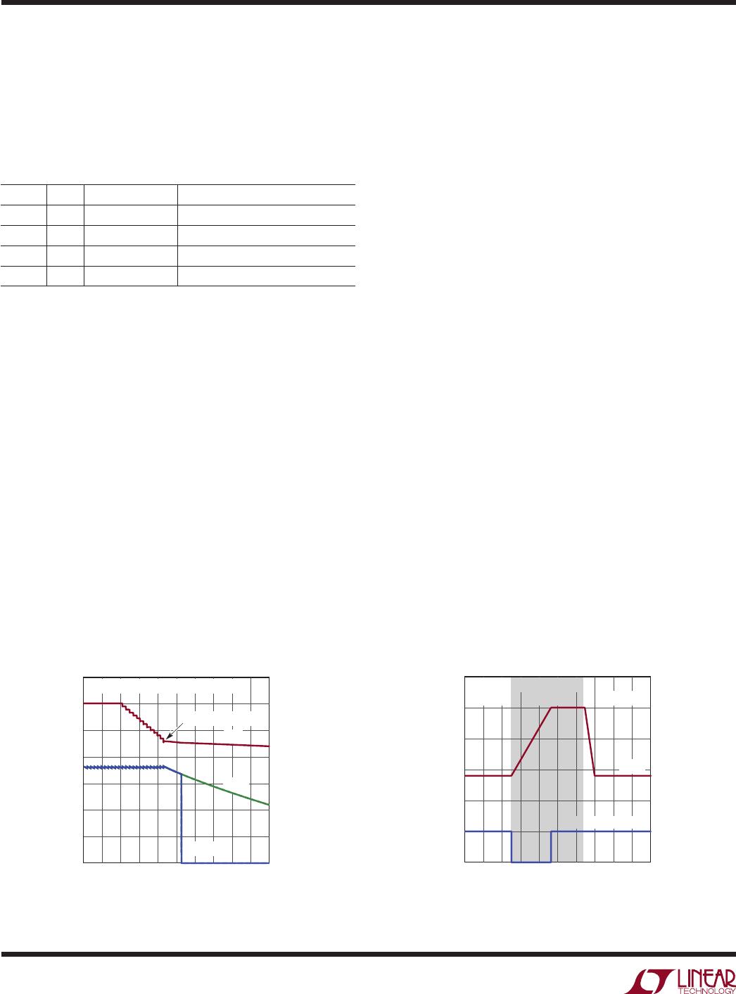
Figure 1. Ideal V
IN
, V
IN2
and CAP Relationship
V
IN
(V)
0
VOLTAGE (V)
18
16
14
12
10
8
6
4
2
0
338813 F01
105 15
V
IN
V
IN2
CAP