LTC3388-1/LTC3388-3
4
338813fa
For more information www.linear.com/LTC3388
ELECTRICAL CHARACTERISTICS
The l denotes the specifications which apply over the full operating
junction temperature range, otherwise specifications are for T
A
= 25°C (Note 2). Unless otherwise noted, V
IN
= 5.5V.
SYMBOL PARAMETER CONDITIONS MIN TYP MAX UNITS
V
IH
D0/D1/EN/STBY Input High Voltage
l
1.2 V
V
IL(D0, D1)
D0/D1 Input Low Voltage
l
0.4 V
V
IL(EN,STBY)
EN/STBY Input Low Voltage
l
150 mV
I
IH
D0/D1/EN/STBY Input High Current 10 nA
I
IL
D0/D1/EN/STBY Input Low Current 10 nA
Additional I
Q
at V
IN
with EN at V
IH(MIN)
V
EN
= 1.2V, V
IN
= 4V 40 nA
Additional I
Q
at V
IN
with STBY at V
IH(MIN)
V
STBY
= 1.2V, V
IN
= 4V 40 nA
Note 1: Stresses beyond those listed under Absolute Maximum Ratings
may cause permanent damage to the device. Exposure to any Absolute
Maximum Rating condition for extended periods may affect device
reliability and lifetime.
Note 2: The LTC
3388-1/LTC3388-3 are tested under pulsed load
conditions such that T
J
≈ T
A
. The LTC3388E-1/LTC3388E-3 are
guaranteed to meet specifications from 0°C to 85°C junction temperature.
Specifications over the –40°C to 125°C operating junction temperature
range are assured by design, characterization and correlation with
statistical process controls. The LTC3388I-1/LTC3388I-3 are guaranteed
over the –40°C to 125°C operating junction temperature range. Note that
the maximum ambient temperature consistent with these specifications
is determined by specific operating conditions in conjunction with board
layout, the rated package thermal impedance and other environmental
factors.
Note 3: The junction temperature (T
J
, in °C) is calculated from the ambient
temperature (T
A
, in °C) and power dissipation (PD, in Watts) according
to the formula: T
J
= T
A
+ (P
D
• θ
JA
), where θ
JA
(in °C/W) is the package
thermal impedance.
Note 4: Dynamic supply current is higher due to gate charge being
delivered at the switching frequency.
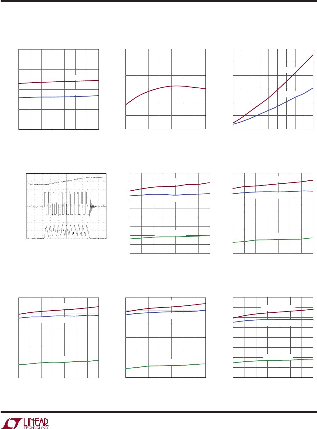
Input I
Q
vs V
IN
, UVLO Input I
Q
vs V
IN
, No Load Input I
Q
vs V
IN
, EN Low
TYPICAL PERFORMANCE CHARACTERISTICS
V
IN
(V)
Q
800
400
500
600
700
300
200
100
0
338813 G01
1 1.5 2 2.50 0.5
–40°C
85°C
25°C
125°C
V
IN
(V)
INPUT I
Q
(nA)
1000
1200
1400
800
600
400
200
338813 G02
6 8 10 202 4 16 1812 14
85°C
25°C
–40°C
125°C
D1 = D0 = 0
V
IN
(V)
Q
1200
800
1000
600
0
200
400
338813 G03
6 8 10 200 2 4 16 1812 14
85°C
25°C
125°C
–40°C