NCP1582, NCP1582A, NCP1583
http://onsemi.com
10
Figure 13. Gain Plot of the Error Amplifier
GAIN (dB)
FREQUENCY (Hz)
100 1000 10 k 100 k 1000 k
Open Loop, Unloaded Gain
Closed Loop,
Unloaded Gain
Error Amplifier
Compensation Network
A
Gain = GMR
1
B
F
Z
F
P
Thermal Considerations
The power dissipation of the NCP158x varies with the
MOSFETs used, V
CC
, and the boost voltage (V
BST
). The
average MOSFET gate current typically dominates the
control IC power dissipation. The IC power dissipation is
determined by the formula:
P
IC
+ (I
CC
@ V
CC
) ) P
TG
) P
BG
.
Where:
P
IC
= control IC power dissipation,
I
CC
= IC measured supply current,
V
CC
= IC supply voltage,
P
TG
= top gate driver losses,
P
BG
= bottom gate driver losses.
The upper (switching) MOSFET gate driver losses are:
P
TG
+ Q
TG
@ f
SW
@ V
BST
.
Where:
Q
TG
= total upper MOSFET gate charge at V
BST
,
f
SW
= the switching frequency,
V
BST
= the BST pin voltage.
The lower (synchronous) MOSFET gate driver losses are:
P
BG
+ Q
BG
@ f
SW
@ V
CC
.
Where:
Q
BG
= total lower MOSFET gate charge at V
CC
.
The junction temperature of the control IC can then be
calculated as:
T
J
+ T
A
) P
IC
@ q
JA
.
Where:
T
J
= the junction temperature of the IC,
T
A
= the ambient temperature,
θ
JA
= the junction−to−ambient thermal resistance of the
IC package.
The package thermal resistance can be obtained from the
specifications section of this data sheet and a calculation can
be made to determine the IC junction temperature. However,
it should be noted that the physical layout of the board, the
proximity of other heat sources such as MOSFETs and
inductors, and the amount of metal connected to the IC,
impact the temperature of the device. Use these calculations
as a guide, but measurements should be taken in the actual
application.
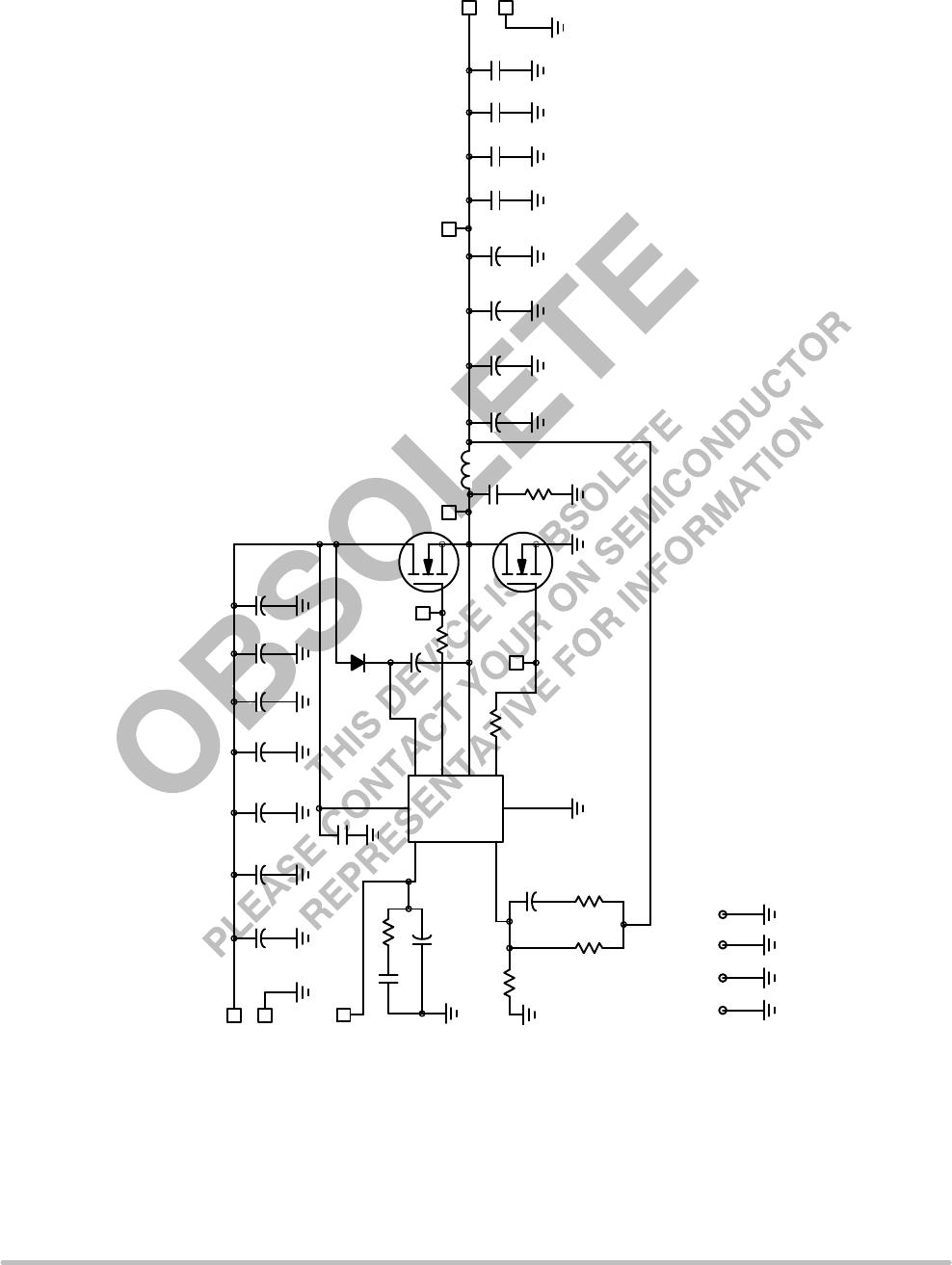
Layout Considerations
As in any high frequency switching converter, layout is
very important. Switching current from one power device to
another can generate voltage transients across the
impedances of the interconnecting bond wires and circuit
traces. These interconnecting impedances should be
minimized by using wide, short printed circuit traces. The
critical components should be located as close together as
possible using ground plane construction or single point
grounding. The figure below shows the critical power
components of the converter. To minimize the voltage
overshoot the interconnecting wires indicated by heavy
lines should be part of ground or power plane in a printed
circuit board. The components shown in the figure below
should be located as close together as possible. Please note
that the capacitors C
IN
and C
OUT
each represent numerous
physical capacitors. It is desirable to locate the NCP158x
within 1 inch of the MOSFETs, Q1 and Q2. The circuit
traces for the MOSFETs’ gate and source connections from
the NCP158x must be sized to handle up to 2 A peak current.
Figure 14. Components to be Considered for
Layout Specifications
PHASE
TG
GND
BG
V
in
RETURN
C
in
L
C
A
D
C
out
V
out
L
out
NCP1582