Complete, High Resolution
16-Bit A/D Converter
ADADC71
Rev. C
Information furnished by Analog Devices is believed to be accurate and reliable.
However, no responsibility is assumed by Analog Devices for its use, nor for any
infringements of patents or other rights of third parties that may result from its use.
Specifications subject to change without notice. No license is granted by implication
or otherwise under any patent or patent rights of Analog Devices. Trademarks and
registered trademarks are the property of their respective owners.
One Technology Way, P.O. Box 9106, Norwood, MA 02062-9106, U.S.A.
Tel: 781.329.4700 www.analog.com
Fax: 781.461.3113 © 2005 Analog Devices, Inc. All rights reserved.
FEATURES
16-bit converter with reference and clock
±0.003% maximum nonlinearity
No missing codes to 14 bits
Fast conversion: 35 μs (14 bit)
Short cycle capability
Parallel logic outputs
Low power: 645 mW typical
Industry standard pinout
APPLICATIONS
Medical and analytic instrumentation
Precision measurement for industrial robots
Automatic test equipment
Multi-channel data acquisition systems
Servo-control systems
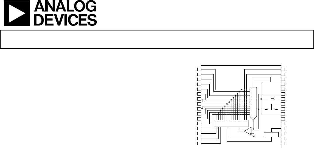
FUNCTIONAL BLOCK DIAGRAM
03537-001
(MSB) BIT 1
1
BIT 2
2
BIT 3
3
BIT 4
4
BIT 5
5
BIT 6
6
BIT 7
7
BIT 8
8
BIT 9
9
BIT 10
10
BIT 11
11
BIT 12
12
(LSB FOR 13 BITS) BIT 13
13
(LSB FOR 14 BITS) BIT 14
14
BIT 15
15
BIT 16
16
SHORT CYCLE
32
CONVERT COMMAND
31
+5V DC SUPPLY V
L
30
GAIN ADJUST
29
+15V DC SUPPLY V
CC
28
COMPARATOR IN
27
BIPOLAR OFFSET
26
+10V
25
+20V
24
REF OUT (4.3V)
23
ANALOG COMMON
22
–15V DC SUPPLY V
EE
21
CLOCK OUT
20
DIGITAL COMMON
19
STATUS
18
NC
NC = NO CONNECT
17
16-BIT DAC
16-BIT SAR
CLOCK
REFERENCE
COMPARATOR
7.5kΩ
3.75kΩ 3.75kΩ
ADADC71
Figure 1.
GENERAL DESCRIPTION
The ADADC71 is a high resolution 16-bit hybrid IC analog-to-
digital converter including reference, clock, and laser-trimmed
thin-film components. The package is a compact 32-pin
hermetic ceramic DIP. The thin-film scaling resistors allow
analog input ranges of ±2.5 V, ±5 V, ±10 V, 0 to +5 V, 0 to +10 V,
and 0 to +20 V.
Important performance characteristics of the device are
maximum linearity error of ±0.003% of FSR, and maximum
conversion time of 50 μs. This performance is due to innovative
design and the use of proprietary monolithic DAC chips. Laser-
trimmed thin-film resistors provide the linearity and wide
temperature range for no missing codes.
The ADADC71 provides data in parallel format with
corresponding clock and status outputs. All digital inputs and
outputs are TTL-compatible. The ADADC71 used to provide
data in a serial format. The serial output function is no longer
available after date code 0120.
PRODUCT HIGHLIGHTS
1. The ADADC71 provides 16-bit resolution with a
maximum linearity error less than ±0.003% (±0.006% for
J grades) at 25
o
C.
2. Conversion time is 35 μs typical (50 μs max) to 14 bits with
short cycle capability.
3. Two binary codes are available on the ADADC71 output:
complementary straight binary (CSB) for unipolar input
voltage ranges, and complementary offset binary (COB) for
bipolar input ranges. Complementary two’s complement
(CTC) coding may be obtained by inverting Pin 1 (MSB).
4. The proprietary chips used in this hybrid design provide
excellent stability over temperature, and lower chip count
for improved reliability.

