ADADC71
Rev. C | Page 9 of 12
Table 6. Input Voltage Range and LSB Values
Analog Input Voltage Range ±10 V ±5 V ±2.5 V 0 V to +10 V 0 V to +5 V
Code Designation COB
1
or CTC
2
COB
1
or CTC
2
COB
1
or CTC
2
CSB
3
CSB
3
One Least Significant Bit (LSB)
n
2
FSR
n
2
V20
n
2
V10
n
2
V5
n
2
V10
n
2
V5
n = 8 78.13 mV 39.06 mV 19.53 mV 39.06 mV 19.53 mV
n = 10 19.53 mV 9.77 mV 4.88 mV 9.77 mV 4.88 mV
n = 12 4.88 mV 2.44 mV 1.22 mV 2.44 mV 1.22 mV
n = 13 2.44 mV 1.22 mV 0.61 mV 1.22 mV 0.61 mV
n = 14 1.22 mV 0.61 mV 0.31 mV 0.61 mV 0.31 mV
n = 15 0.61 mV 0.31 mV 0.15 mV 0.31 mV 0.15 mV
1
COB = complementary offset binary.
2
CTC = complementary twos complement—achieved by using an inverter to complement the most significant bit to produce (MSB).
3
CSB = complementary straight binary.
03537-011
–15V
+15V
A
16-BIT SUCCESSIVE
APPROMIXATION REGISTER
16-BIT DAC
REF
CONTROL
3.75kΩ3.75kΩ
242619
29
28
22
21
25
e
IN
(0V TO +10V)
I
IN
KEEP/
REJECT
7.5kΩ
+15V
–15V
ZERO
ADJ
10kΩ
TO
100kΩ
27
I
OS
= 1.3mA
ADADC71
1.8MΩ
1μF
+5V
+
30
+
1μF
+
1μF
+15V
–15V
GAIN
ADJ
10kΩ
TO
100
k
Ω
270kΩ
0.01μF
NOTE:
A
NALOG ( ) AND DIGITAL ( ) GROUNDS ARE NOT TIED INTERNALLY AND MUST BE CONNECTED EXTERNALLY
.
23
Figure 11. Analog and Power Connections
for Unipolar 0 V to +10 V Input Range
03537-012
–15V
+15V
A
16-BIT SUCCESSIVE
APPROMIXATION REGISTER
16-BIT DAC
REF
CONTROL
3.75kΩ3.75kΩ
242619
29
28
22
21
25
e
IN
(–10V TO +10V)
I
IN
KEEP/
REJECT
7.5kΩ
+15V
–15V
ZERO
ADJ
10kΩ
TO
100kΩ
27
I
OS
= 1.3mA
ADADC71
1.8MΩ
1μF
+5V
+
30
+
1μF
+
1μF
+15V
–15V
GAIN
ADJ
10kΩ
TO
100
k
Ω
270kΩ
0.01μF
NOTE:
A
NALOG ( ) AND DIGITAL ( ) GROUNDS ARE NOT TIED INTERNALLY AND MUST BE CONNECTED EXTERNALLY
.
23
Figure 12. Analog and Power Connections
for Bipolar −10 V to +10 V Input Range
CALIBRATION (14-BIT RESOLUTION EXAMPLES)
External zero adjustment and gain adjustment potentiometers,
connected as shown in
Figure 5 and Figure 6, are used for
device calibration. To prevent interaction of these two
adjustments, zero is always adjusted first and then gain. Zero is
adjusted with the analog input near the most negative end of the
analog range (0 for unipolar and −FS for bipolar input ranges).
Gain is adjusted with the analog input near the most positive
end of the analog range.
0 V to +10 V Range
Set the analog input to +1 LSB
14
= 0.00061 V. Adjust zero for
digital output = 11111111111110. Zero is now calibrated. Set
analog input to +FSR − 2 LSB = +9.9987 V. Adjust gain for
00000000000001 digital output code; full-scale (gain) is now
calibrated. Half-scale calibration check: set analog input to
+5.00000 V; digital output code should be 01111111111111.
−10 V to +10 V Range
Set the analog input to −9.99878 V; adjust zero for
11111111111110 digital output (complementary offset binary)
code. Set analog input to 9.99756 V; adjust gain for
00000000000001 digital output (complementary offset binary)
code. Half-scale calibration check: set analog input to 0.00000
V; digital output (complementary offset binary) code should be
01111111111111.
Other Ranges
Representative digital coding for 0 to +10 V and −10 V to +10 V
ranges is given above. Coding relationships and calibration
points for 0 to +5 V, −2.5 V to +2.5 V and −5 V to +5 V ranges
can be found by proportionally halving the corresponding code
equivalents listed for the 0 to +10 V and −10 V to +10 V ranges,
respectively, as indicated in
Tabl e 5.
Zero and full-scale calibration can be accomplished to a
precision of approximately ±1/2 LSB using the static adjustment
procedure described above. By summing a small sine or
triangular wave voltage with the signal applied to the analog
input, the output can be cycled through each of the calibration
codes of interest to more accurately determine the center (or
end point) of each discrete quantization level. A detailed
description of this dynamic calibration technique is presented
in
A/D Conversion Handbook, D. Sheingold, Analog Devices,
Inc., 1986 Part II, Chapter 4.
ADADC71
Rev. C | Page 10 of 12
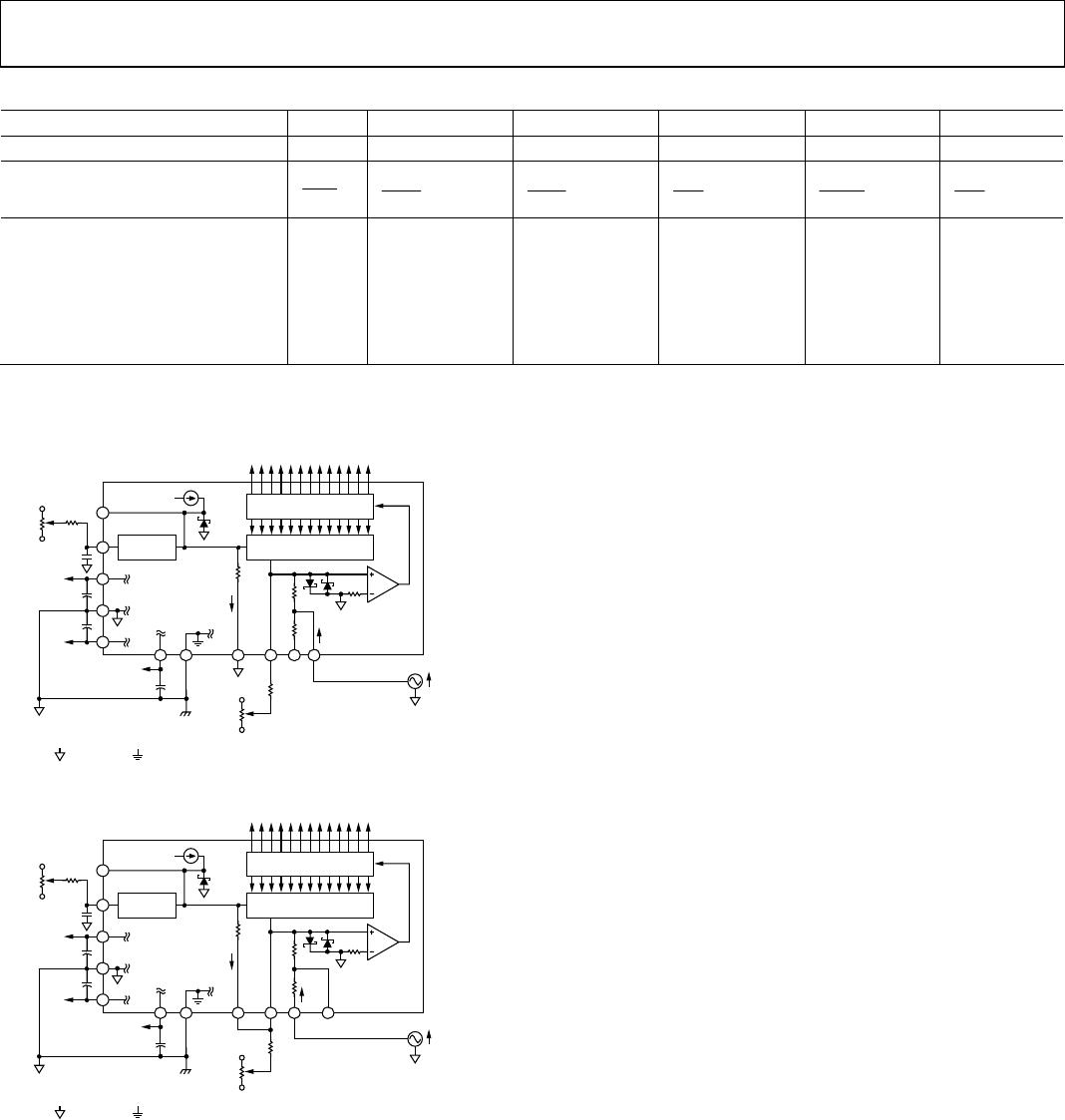
GROUNDING, DECOUPLING, AND LAYOUT
CONSIDERATIONS
Many data-acquisition components have two or more ground
pins, which are not connected together within the device. These
grounds are usually referred to as the DIGITAL COMMON
(logic power return), ANALOG COMMON (analog power
return), or analog signal ground. These grounds (Pin 19 and
Pin 22) must be tied together at one point as close as possible to
the converter. Ideally, a single solid analog ground plane under
the converter would be desirable. Current flows through the
wires and etch stripes of the circuit card, and since these paths
have resistance and inductance, hundreds of millivolts can be
generated between the system analog ground point and the
ground pins of the ADADC71. Separate wide conductor stripe
ground returns should be provided for high resolution
converters to minimize noise and IR losses from the current
flow in the path from the converter to the system ground point.
In this way the ADADC71 supply currents and other digital
logic-gate return currents are not summed into the same return
path as analog signals where they would cause measurement
errors.
Each of the ADADC71’s supply terminals should be capacitively
decoupled as close to the ADADC71 as possible. A large value,
such as 1 μF, capacitor in parallel with a 0.1 μF capacitor is
usually sufficient. Analog supplies are to be bypassed to the
ANALOG COMMON (analog power return) Pin 22 and the
logic supply is bypassed to DIGITAL COMMON (logic power
return) Pin 19.
The metal cover is internally grounded with respect to the
power supplies, grounds and electrical signals. Do not
externally ground the cover.
T/H REQUIREMENTS FOR HIGH RESOLUTION
APPLICATIONS
The characteristics required for high resolution track-and-hold
amplifiers are low feedthrough, low pedestal shifts with changes
of input signal or temperature, high linearity, low temperature
coefficients, and minimal droop rate.
The aperture jitter is a result of noise within the switching
network that modulates the phase of the hold command, and is
manifested in the variations in the value of the analog input that
has been held. The aperture error which results from this jitter
is directly related to the dV/dt of the analog input.
The T/H amplifier slew rate determines the maximum
frequency tracking rate and part of the settling time when
sampling pulses and square waves. The feedthrough from input
to output while in the hold mode should be less than 1 LSB. The
amplitude of 1 LSB of the companion ADC for a given input
range will vary from 610 μV for a 14-bit ADC using a 0 V to
+10 V input range to 4.88 mV for a 12-bit ADC using a ±10 V
input range. The hold mode droop rate should produce less
than 1 LSB of droop in the output during the conversion time of
the ADC. For 610 μV/LSB, as noted in the example above, for a
50 μs 14-bit ADC, the maximum droop rate is 610 μV/50 μs or
12 μV/μs during the 50 μs conversion period.
Minimal thermal tail effects are another requirement of high
resolution applications. The self-heating errors induced by the
changing current levels in the output stages of T/H amps may
cause more than 1 LSB of error due to thermal tail effects.
The linearity error should be less than 1 LSB over the transfer
function, as set by the resolution of the ADC. The T/H
acquisition time and T/H settling time along with the
conversion time of the ADC determines the highest sampling
rate. This in turn determines the highest input signal frequency
that can be sampled at twice a cycle.
The maximum input frequency is constrained by the Nyquist
sampling theorem to be half of the maximum throughput rate.
Input frequencies higher than half the maximum throughput
rate result in under sampling or aliasing errors of the input
signal.
The pedestal shift due to input signal changes should either be
linear, to be seen as a gain error, or negligible, as with the
feedthrough specification. The temperature coefficients for drift
would be low enough such that full accuracy is maintained over
some minimum temperature range. The droop rate and
pedestal shift increases above +70
o
C (+158
o
F). For commercial
and industrial users, these shifts only appear above the highest
temperatures their equipment might expect to experience. Most
precision instrumentation is installed only in human
inhabitable work spaces or in controlled enclosures if the area
has a hostile environment. Thus, the ADADC71 used with a
sample-and-hold amplifier offers high accuracy sampling in
high precision applications.
ADADC71
Rev. C | Page 11 of 12
USING THE ADADC71 AT SLOWER CONVERSION
TIMES
The user may wish to run the ADADC71 at slower conversion
times in order to synchronize the ADC with an external clock.
This is accomplished by running a slower clock that the internal
clock into the START CONVERT input. This clock must consist
of narrow negative-going clock pulses, as seen in
Figure 13. The
pulse must be a minimum of 100 ns wide, but not greater than
700 ns. Having a raising edge immediately after a falling edge
inhibits the internal clock pulse. This enables the ADADC71 to
function normally and complete a conversion after 16 clock
pulses. The STATUS command functions normally and
switches high after the first clock pulse and falls low after the
17
th
clock pulse. In this way an external clock can be used to
control the ADADC71 at slower conversion times.
03537-013
START CONVERT
(EXTERNAL CLOCK)
CLOCK OUT
STATUS
100ns MIN
1500ns MAX
1
t
1
t
15
t
16
t
0
NOTE:
1
EXTENAL CLK RATE CTRL (PIN 23) GROUNDED.
Figure 13. Timing Diagram for Use with an External Clock

ADADC71JD

Mfr. #:
Manufacturer:
Analog Devices Inc.
Description:
Analog to Digital Converters - ADC High Resolution 16B
Lifecycle:
New from this manufacturer.
Delivery:
DHL FedEx Ups TNT EMS
Payment:
T/T Paypal Visa MoneyGram Western Union

Products related to this Datasheet