ADADC71
Rev. C | Page 6 of 12
THEORY OF OPERATION
The analog continuum is partitioned into 2
16
discrete ranges for
16-bit conversion. All analog values within a given quantum are
represented by the same digital code, usually assigned to the
nominal midrange value. An inherent quantization uncertainty
of ±1/2 LSB is associated with the resolution, in addition to the
actual conversion errors.
0.016
0.013
0.0195
0.0150
0.0180
0
–0.0150
–0.0180
–0.0195
0.006
0.003
0
–0.003
–0.006
–0.016
–0.013
025 70
03537-002
TEMPERATURE (°C)
LINEARITY ERROR (% FSR)
ADADC71
±3ppm/°C,
±0.006%, @ 25°C
Figure 2. Linearity Error vs. Temperature
0.100
0.038
–0.038
0
–0.068
0.068
0
–0.100
0605040302010
03537-003
TEMPERATURE (°C)
GAIN DRIFT ERROR (% FSR)
70
±15ppm/°C
Figure 3. Gain Drift Error vs. Temperature
The actual conversion errors associated with ADCs are
combinations of analog errors due to the linear circuitry,
matching and tracking properties of the ladder and scaling
networks, reference error, and power supply rejection. The
matching and tracking errors in the converter have been
minimized by the use of monolithic DACs that include the
scaling network. The initial gain and offset errors are specified
at ±0.2% FSR for gain and ±0.1% FSR for offset. These errors
may be trimmed to 0 by using external trim circuits as shown in
Figure 5 and Figure 6. Linearity error is defined for unipolar
ranges as the deviation from a true straight-line transfer
characteristic from a zero voltage analog input, which calls for a
zero digital output, to a point that is defined as a full scale. The
linearity error is based on the DAC resistor ratios. It is
unadjustable and is the most meaningful indication of ADC
accuracy. Differential nonlinearity is a measure of the deviation
in the staircase step width between codes from the ideal least
significant bit step size (
Figure 4).
03537-004
000 ... 000
ALL BITS ON
GAIN
ERROR
OFFSET
ERROR
ALL BITS OFF
–1/2LSB
+1/2LSB
011 ... 111
111 ... 111
DIGITAL OUTPUT (COB CODE)
–FS
ANALOG INPUT
0
+FSR – 1LSB
Figure 4. Transfer Characteristics for an Ideal Bipolar ADC
Monotonic behavior requires that the differential linearity error
be less than 1 LSB. However, a monotonic converter can have
missing codes. The ADADC71 is specified as having no missing
codes over temperature ranges noted in the
Specifications
section.
There are three types of drift error over temperature: offset, gain
and linearity. Offset drift causes a shift of the transfer
characteristic left or right on the diagram over the operating
temperature range. Gain drift causes a rotation of the transfer
characteristic about the zero point for unipolar ranges or the
negative full-scale point for bipolar ranges. The worst case
accuracy drift is the summation of all three drift errors over
temperature. Statistically, however, the drift error behaves as the
root-sum-square (RSS) and can be shown as
222
L
OG
RSS ++=
where:
)./( Cppmerrordriftgain
G
°
=
)./( CFSRofppmerrordriftoffset
O
°
=
)./( CFSRofppmerrorlinearity
L
°
=
ADADC71
Rev. C | Page 7 of 12
DESCRIPTION OF OPERATION
On receipt of a CONVERT START command, the ADADC71
converts the voltage at its analog input into an equivalent 16-bit
binary number. This conversion is accomplished as follows: the
16-bit successive-approximation register (SAR) has its 16-bit
outputs connected both to the device bit output pins and to the
corresponding bit inputs of the feedback DAC. The analog
input is successively compared to the feedback DAC output, one
bit at a time (MSB first, LSB last). The decision to keep or reject
each bit is then made at the completion of each bit comparison
period, depending on the state of the comparator at that time.
GAIN ADJUSTMENT
The gain adjustment circuit consists of a 100 ppm/
o
C poten-
tiometer connected across ±V
S
with its slider connected
through a 510 kΩ resistor to Pin 29 (GAIN ADJUST), as shown
in
Figure 5.
If no external trim adjustment is desired, Pin 27
(COMPARATOR IN) and Pin 29 may be left open.
03537-005
ADADC71
29
0.01μF
270kΩ
+15V
10kΩ
TO
100kΩ
100ppm/°C
–15V
Figure 5. Gain Adjustment Circuit
ZERO OFFSET ADJUSTMENT
The zero offset adjustment circuit consists of a 100 ppm/
o
C
potentiometer connected across ±V
S
with its slider connected
through a 1.8 MΩ resistor to Pin 27 for all ranges. As shown in
Figure 6, the tolerance of this fixed resistor is not critical; a
carbon composition type is generally adequate. Using a carbon
composition resistor with a −1200 ppm/
o
C temperature
coefficient contributes a worst-case offset temperature
coefficient of 32 LSB
B
14
× 61 ppm/ LSB
14
× 1200 ppm/ C =
2.3 ppm/ C of FSR, if the offset adjustment potentiometer is set
at either end of its adjustment range. Since the maximum offset
adjustment required is typically no more than ±16 LSB
o
o
14
, use of
a carbon composition offset summing resistor typically
contributes no more than 1 ppm/ C of FSR offset temperature
coefficient.
o
03537-006
ADADC71
27
1.8MΩ
+15V
10kΩ
TO
100kΩ
–15V
Figure 6. Zero Offset Adjustment Circuit
An alternate offset adjustment circuit, which contributes
negligible offset temperature coefficient if metal film resistors
(temperature coefficient < 100 ppm/
o
C) are used, is shown in
Figure 7.
In either adjustment circuit, the fixed resistor connected to
Pin 27 should be located close to this pin to keep the pin
connection runs short. Pin 27 is quite sensitive to external noise
pick-up.
03537-007
ADADC71
27
22kΩ M.F.
180kΩ M.F.
180kΩ M.F.
+15V
10kΩ
TO
100kΩ
OFFSET
ADJ
–15V
Figure 7. Low Temperature Coefficient Zero Adjustment Circuit
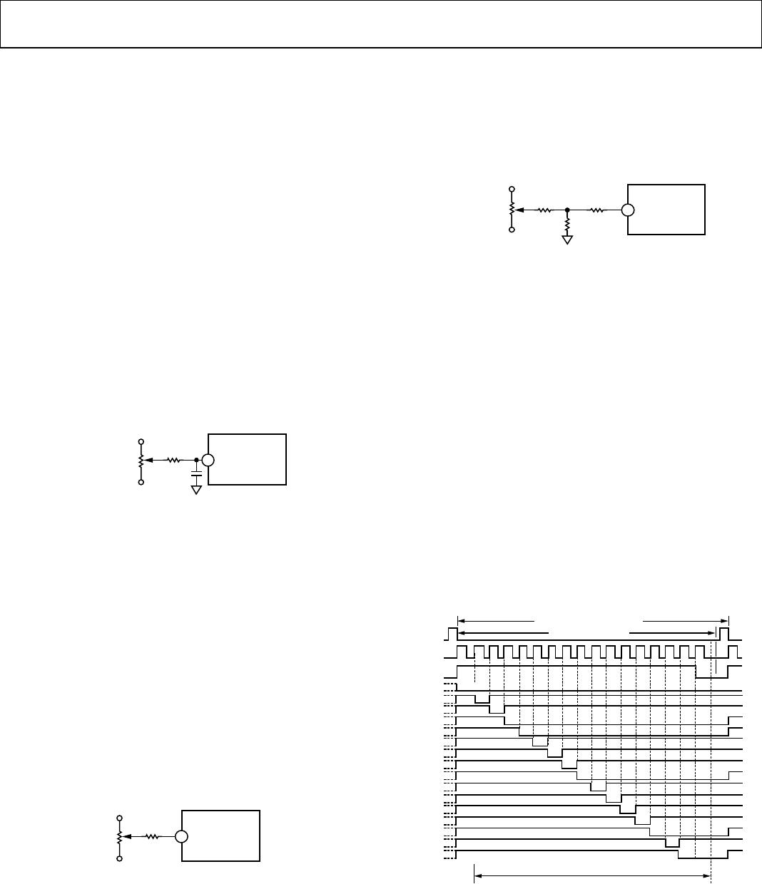
TIMING
The timing diagram is shown in Figure 8. Receipt of a
CONVERT START signal sets the STATUS flag, indicating
conversion in progress. This in turn removes the inhibit applied
to the gated clock, permitting it to run through 17 cycles. All
the SAR parallel bits, STATUS flip-flops, and the gated clock
inhibit signal are initialized on the trailing edge of the
CONVERT START signal. At time t
0
, B
1
is reset and B
2
to B
16
are
set unconditionally. At t
1
the Bit 1 decision is made (keep) and
Bit 2 is reset unconditionally. This sequence continues until the
Bit 16 (LSB) decision (keep) is made at t
16
. The STATUS flag is
reset, indicating that the conversion is complete and that the
parallel output data is valid. Resetting the STATUS flag restores
the gated clock inhibit signal, forcing the clock output to the
low Logic 0 state. Note that the clock remains low until the next
conversion.
Corresponding parallel data bits become valid on the same
positive-going clock edge.
03537-008
t
0
t
1
t
2
t
3
t
4
t
5
t
6
t
7
t
8
t
9
t
10
t
11
t
12
t
13
t
14
t
15
t
16
t
17
(4)
(3)
(1)
01 1 0 01 110 1 11 1 0 10
0
1
1
0
0
1
1
1
0
1
1
1
1
0
1
0
MSB
STATUS
INTERNAL
CLOCK
CONVERT
START
BIT 2
BIT 3
BIT 4
BIT 5
BIT 6
BIT 7
BIT 8
BIT 9
BIT 10
BIT 11
BIT 12
BIT 13
BIT 14
BIT 15
LSB
LSBMSB
MAXIMUM THROUGHPUT TIME
CONVERSION TIME (2)
NOTES:
1. THE CONVERT START PULSEWIDTH IS 50ns MIN AND MUST REMAIN LOW DURING A
CONVERSION. THE CONVERSION IS INITIATED BY THE TRAILING EDGE OF THE
CONVERT COMMAND.
2. 50μs FOR 14 BITS AND 45μs FOR 13 BITS (MAX).
2. MSB DECISION.
3. CLOCK REMAINS LOW AFTER LAST BIT DECISION.
Figure 8. Timing Diagram (Binary Code 0110011101111010)
ADADC71
Rev. C | Page 8 of 12
DIGITAL OUTPUT DATA
Parallel data from TTL storage registers is in negative true form
(Logic 1 = 0 V and Logic 0 = 2.4 V). Parallel data output coding
is complementary binary for unipolar ranges and comple-
mentary offset binary for bipolar ranges. Parallel data becomes
valid at least 20 ns before the STATUS flag returns to Logic 0,
permitting parallel data transfer to be clocked on the 1 to 0
transition of the STATUS flag (see
Figure 9). Parallel data
outputs change state on positive-going clock edges.
03537-009
BIT 16
VALID
BUSY
(STATUS)
20ns MIN TO 90ns
Figure 9. LSB Valid to Status Low
Short Cycle Input: Pin 32 (SHORT CYCLE) permits the timing
cycle shown in Figure 8 to be terminated after any number of
desired bits has been converted, allowing somewhat shorter
conversion times in applications not requiring full 16-bit
resolution. When 10-bit resolution is desired, Pin 32 is
connected to Bit 11 output Pin 11. The conversion cycle then
terminates and the STATUS flag resets after the Bit 10 decision
(t
10
+ 40 ns in the timing diagram of Figure 8). Short cycle
connections and associated maximum 8-, 10-, 12-, 13-, 14-, and
15-bit conversion times are summarized in
Tabl e 3.
Table 3. Short Cycle Connections
Resolution
Connect Short
Cycle Pin 32
to
Bits % FSR
Maximum
Conversion
Time
Status
Flag
Reset
N/C (Open) 16 0.0015 57.0 t
16
+ 40 ns
Pin 16 15 0.003 53.5 t
15
+ 40 ns
Pin 15 14 0.006 50.0 t
14
+ 40 ns
Pin 14 13 0.012 46.5 t
13
+ 40 ns
Pin 13 12 0.024 42.8 t
12
+ 40 ns
Pin 11 10 0.100 35.6 t
10
+ 40 ns
Pin 9 8 0.390 28.5 t
8
+ 40 ns
INPUT SCALING
The ADADC71 inputs should be scaled as close to the
maximum input signal range as possible in order to utilize the
maximum signal resolution of the ADC. Connect the input
signal as shown in
Table 4. See Figure 10 for circuit details.
03537-010
22
ANALOG
COMMON
26
BIPOLAR
OFFSET
COMP IN
24
25
27
7.5kΩ
R2
3.75kΩ
10V SPAN
20V SPAN
R1
3.75kΩ
FROM DAC
COMPARATOR
TO
SAR
V
REF
Figure 10. ADADC71 Input Scaling Circuit
Table 4. Input Scaling Connections
Input Signal Line Output Code Connect Pin 26 to Connect Pin 24 to
For Direct Input,
Connect Input Signal to
±10 V COB Pin 27
1
Input Signal Pin 24
±5 V COB Pin 27
1
Open Pin 25
±2.5 V COB Pin 27
1
Pin 27
1
Pin 25
0 V to +5 V CSB Pin 22 Pin 27
1
Pin 25
0 V to +10 V CSB Pin 22 Open Pin 25
0 V to +20 V CSB Pin 22 Input Signal Pin 24
1
Pin 27 is extremely sensitive to noise and should be guarded by analog common
Table 5. Transition Values vs. Calibration Codes
Output Code
MSB LSB
1
Range ±10 V ±5 V ±2.5 V 0 V to +10 V 0 V to +5 V
000. . . .000
2
+Full Scale +10 V +5 V +2.5 V +10 V +5 V
−3/2 LSB −3/2 LSB −3/2 LSB −3/2 LSB −3/2 LSB
011 . . . 111 Mid Scale 0 0 0 +5 V +2.5 V
−1/2 LSB −1/2 LSB −1/2 LSB −1/2 LSB −1/2 LSB
111 . . . 110 −Full Scale −10 V −5 V −2.5 V 0 V 0 V
+1/2 LSB +1/2 LSB +1/2 LSB +1/2 LSB +1/2 LSB
1
For LSB value for range and resolution used, see Table 6.
2
Voltages given are the nominal value for transition to the code specified.

ADADC71JD

Mfr. #:
Manufacturer:
Analog Devices Inc.
Description:
Analog to Digital Converters - ADC High Resolution 16B
Lifecycle:
New from this manufacturer.
Delivery:
DHL FedEx Ups TNT EMS
Payment:
T/T Paypal Visa MoneyGram Western Union

Products related to this Datasheet