ADADC71
Rev. C | Page 4 of 12
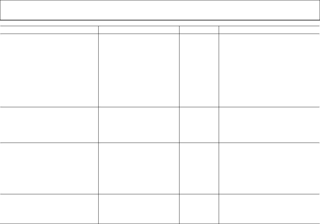
Parameter Min Typ Max Units Comment
DIGITAL OUTPUT
1
All codes complementary
Parallel Output Codes
6
Unipolar CSB
Bipolar COB, CTC
7
Output Drive 5 LSTTL Loads
Status Logic 1 during conversion
Status Output Drive 5 LSTTL Loads
Internal Clock
Clock Output Drive 5 LSTTL Loads
Frequency 400 kHz
INTERNAL REFERENCE VOLTAGE 6.3 V dc
Error ±5 %
Max External Current Drain with No
Degradation of Specifications
±200 μA
Temperature Coefficient ±10 ppm/
o
C
POWER SUPPLY REQUIREMENTS
Power Consumption 645 850 mW
Rated Voltage, Analog ±15 ±0.5 V dc
Rated Voltage, Digital ±5 ±0.25 V dc
Supply Drain +15 V dc +16 mA
Supply Drain −15 V dc −21 mA
Supply Drain +5 V dc +18 mA
TEMPERATURE RANGE
Specification 0 to +70 °C
Operating (Derated Specs) −25 to +85 °C
Storage −55 to +125 °C
1
For inputs Logic 0 = 0.8 V, max. Logic 1 = 2.0 V, min. For digital outputs Logic 0 = 0.4 V max. Logic 1 = 2.4 V min.
2
Adjustable to 0.
3
Full scale range.
4
For definition of “No Missing Codes,” refer to the Theory of Operation section.
5
Conversion time may be shortened with short cycle set for lower resolution.
6
CSB—Complementary straight binary. COB— Complementary offset binary, CTC—Complementary twos complement.
7
CTC coding obtained by inverting MSB (Pin 1).