MAX2306/MAX2308/MAX2309
CDMA IF VGAs and I/Q Demodulators
with VCO and Synthesizer
______________________________________________________________________________________ 11
M
S
B
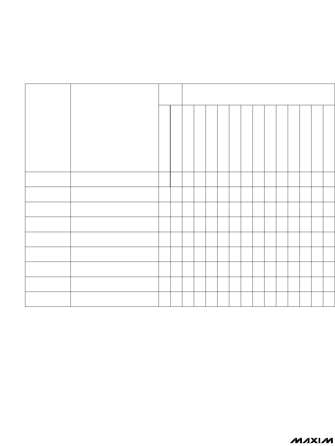
Table 2. MAX2308 Control Register States
Note: H = high, L = low, 1 = logic high, 0 = logic low, X = don’t care, blank = independent parameter
STBY
OPERATIONAL
MODE
11 10X X0FM_I FM I operation 0H
10 10X X0FM_IQ FM IQ quadrature operation 0H
1X 11X X0CDMA CDMA operation 0H
0 1X X0STANDBY
0 in standby pin turns off VGA and
modulator only
0H
XX LXX XXX XSHUTDOWN
0 in shutdown register bit leaves seri-
al port active
XH X XX
XX X
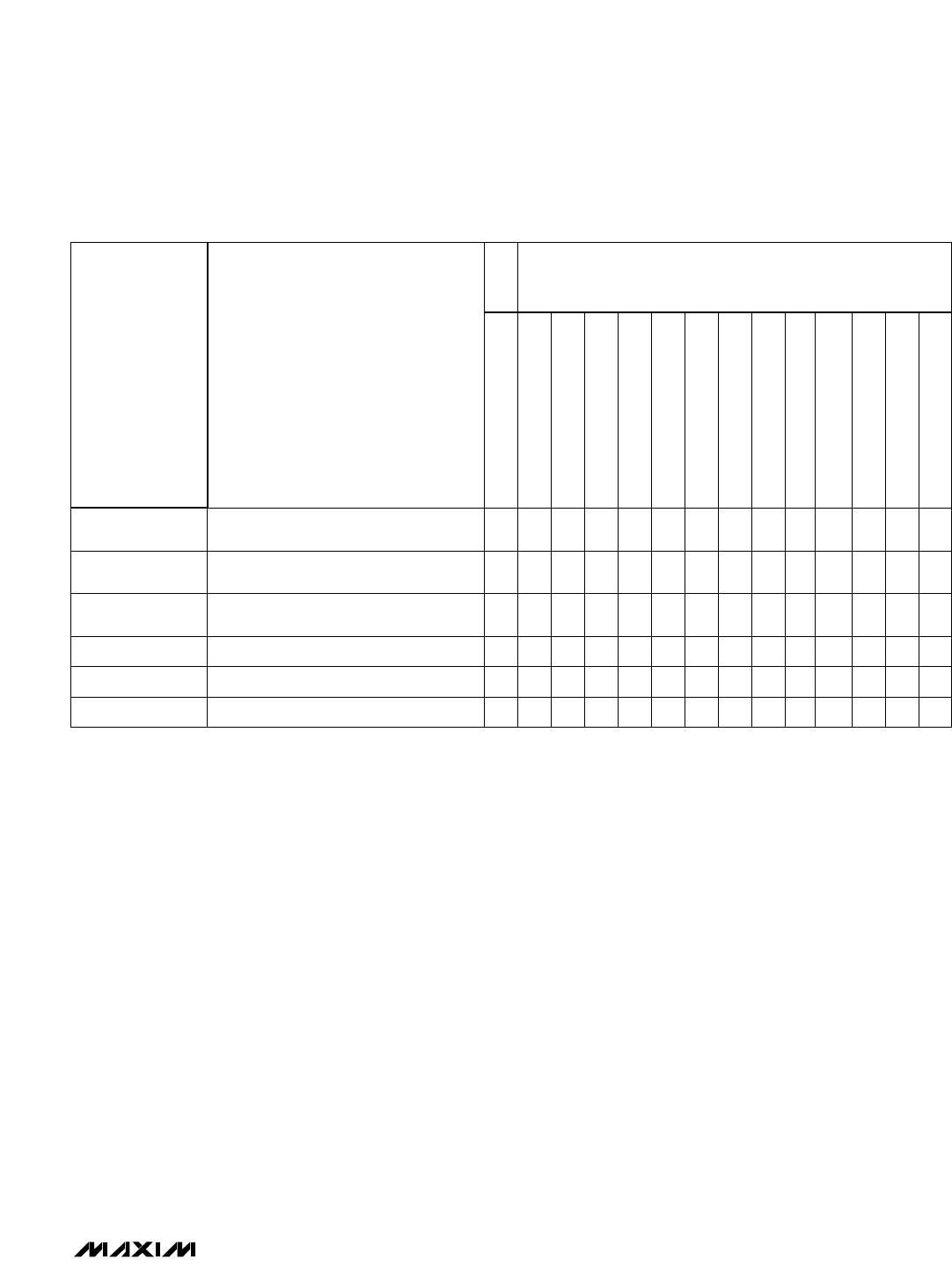
ML
S CONTROL REGISTER S
BB
SHDN
X
IN_SEL
FM_TYPE
X X
BUFEN
BUF_DIV
XX X
VCO_SEL
VCO_BYP
SHUTDOWN
Shutdown pin completely shuts down
chip
DIVSEL
XL X X
TURBOCHARGE
TEST_EN
X
CP_POL
P
I
N
SHDN
TEST_MODE
ACTION
RESULT
When the part initially powers up or changes state, the
synthesizer acquisition time can be reduced by using
the Turbo feature, enabled by the TURBOCHARGE
(TC) control bit. Turbo functionality provides a larger
charge-pump current during acquisition mode. Once
the VCO frequency is acquired, the charge-pump out-
put current magnitude automatically returns to the pre-
programmed state to maintain loop stability and
minimize spurs in the VCO output signal.
The lock detect output indicates when the PLL is
locked with a logic high.
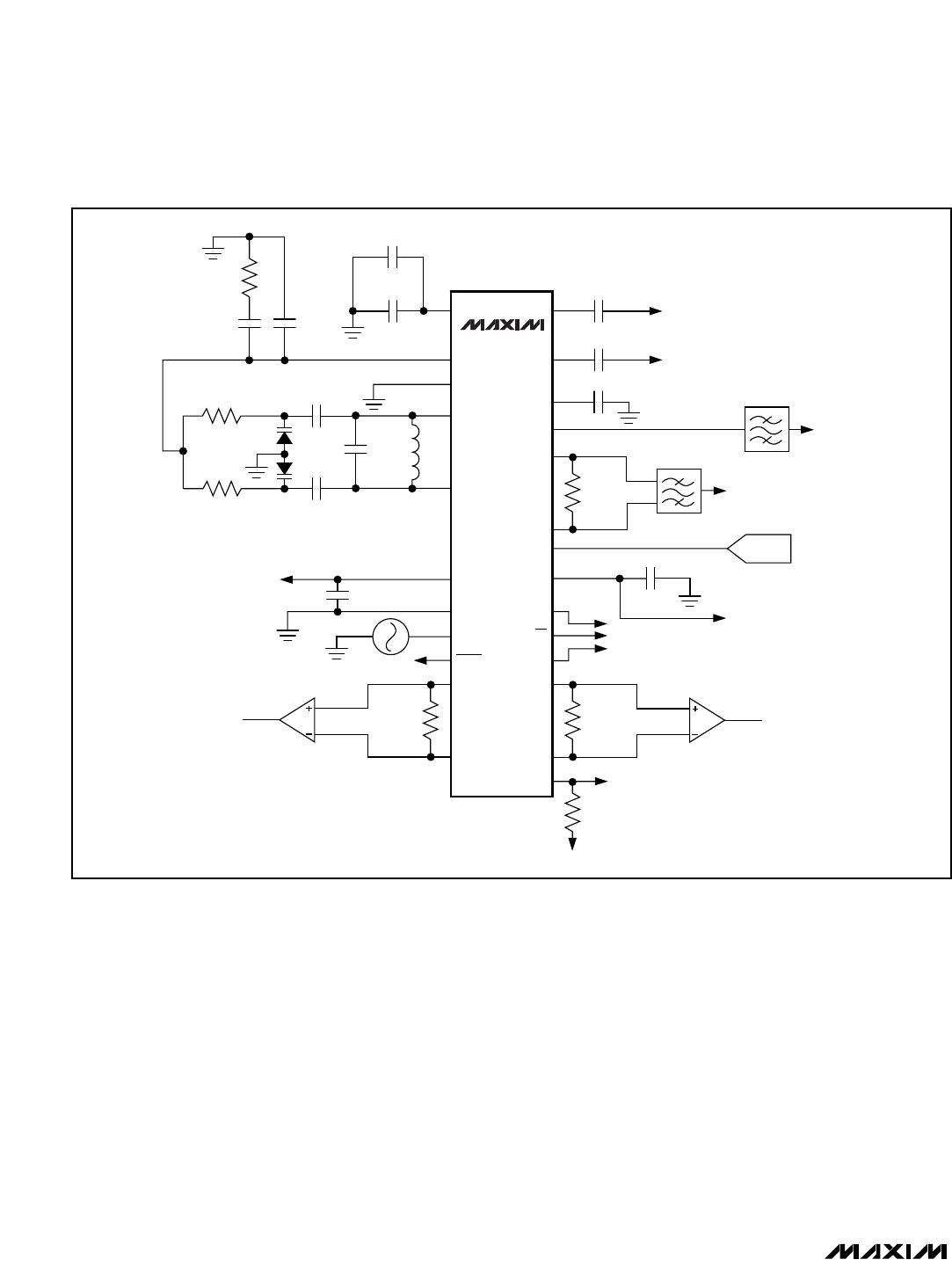
3-Wire Interface and Registers
The MAX2306 family incorporates a 3-wire interface for
synthesizer programming and device configuration
(Figure 5). The 3-wire interface consists of clock, data,
and enable signals. It controls the VCO dividers (M1
and M2), reference frequency dividers (R1 and R2),
and a 13-bit control register. The control register is
used to set up the operational modes (Table 4). The
input shift is 17 data bits long and requires a total of 18
clock bits (Figure 6). A single clock pulse is required
before enable drops low to initialize the data bus.
Whenever the M or R divide register value is pro-
grammed and downloaded, the control register must
also be subsequently updated. This prevents turbolock
from going active when not desired.
The SHDN control bit is notable because it differs from
the SHDN pin. When the SHDN control bit is low, the
registers and serial interface are left active, retaining
the values stored in the latches, while the rest of the
device is shut off. In contrast, the SHDN pin, when low,
shuts down everything, including the registers and seri-
al interface. See Functional Diagram.
Registers
Figure 7 shows the programming logic. The 17-bit shift
register is programmed by clocking in data at the rising
edge of CLK. Before the shift register is able to accept
data, it must be initialized by driving it with at least one
full clock cycle at the CLK input with EN high (see
Figure 6). Pulling enable low will allow data to be
clocked into the shift register; pulling enable high loads
the register addressed by A0, A1, and A2, respectively
(Figure 7). Table 5 lists the power-on default values of
all registers. Table 6 lists the charge-pump current,
depending on CP0 and CP1.