MAX2306/MAX2308/MAX2309
CDMA IF VGAs and I/Q Demodulators
with VCO and Synthesizer
_______________________________________________________________________________________ 7
Pin Description
PIN
MAX2306
MAX2308 MAX2309
NAME FUNCTION
1, 28
TANKL+,
TANKL-
Differential Tank Input for Low-Frequency Oscillator
1, 4 N.C. No Connection. Must be left open-circuit.
2, 3 2, 3 1, 2
TANKH+,
TANKH-
Differential Tank Input for High-Frequency Oscillator
—— 3BUFEN LO Buffer Amplifier—active low
4 MODE Mode Select. High selects CDMA mode; low selects FM mode.
4 LOOUT
Internal VCO Output. Depending on setting of BD bit, LOOUT is
either the VCO frequency (twice the IF frequency) or one-half the
VCO frequency (equal to the IF frequency).
555V
CC
+2.7V to +5.5V Supply
6 6 6 GND Ground
7 7 7 REF Reference Frequency Input
888SHDN
Shutdown Input—active low. Low powers down entire device,
including registers and serial interface.
9, 10 9, 10 9, 10
IOUT+,
IOUT-
Differential In-Phase Baseband Output, or FM signal output if FM_I
mode is selected.
11 11 11 LOCK
Lock Output—open-collector pin. Logic high indicates phase-locked
condition.
12, 13 12, 13 12, 13
QOUT-,
QOUT+
Differential Quadrature-Phase Baseband Output. Disabled if FM_I
mode is selected.
14 14 14 CLK Clock input of the 3-wire serial bus
15 15 15 EN Enable Input. When low, input shift register is enabled.
16 16 16 DATA Data input of the 3-wire serial bus.
17 17 17 V
CC
+2.7V to +5.5V Supply
18 18 18 VGC VGA Gain Control Input. Control voltage range is 0.5V to 2.3V.
19, 20 19, 20 19, 20
CDMA-,
CDMA+
Differential CDMA Input. Active in CDMA mode.
21 21 FM+ Differential Positive Input. Active in FM mode.
22 22 FM-
Differential Negative Input for FM signal. Bypass to GND for
single-ended operation.
——22STBY
Standby Input—active low. Low powers down VGA and demodulator
while keeping VCO, PLL, and serial bus on.
23, 24 23, 24 23, 24 BYP Bypass Node. Must be capacitively decoupled (bypassed) to pin 17.
MAX2306/MAX2308/MAX2309
CDMA IF VGAs and I/Q Demodulators
with VCO and Synthesizer
8 _______________________________________________________________________________________
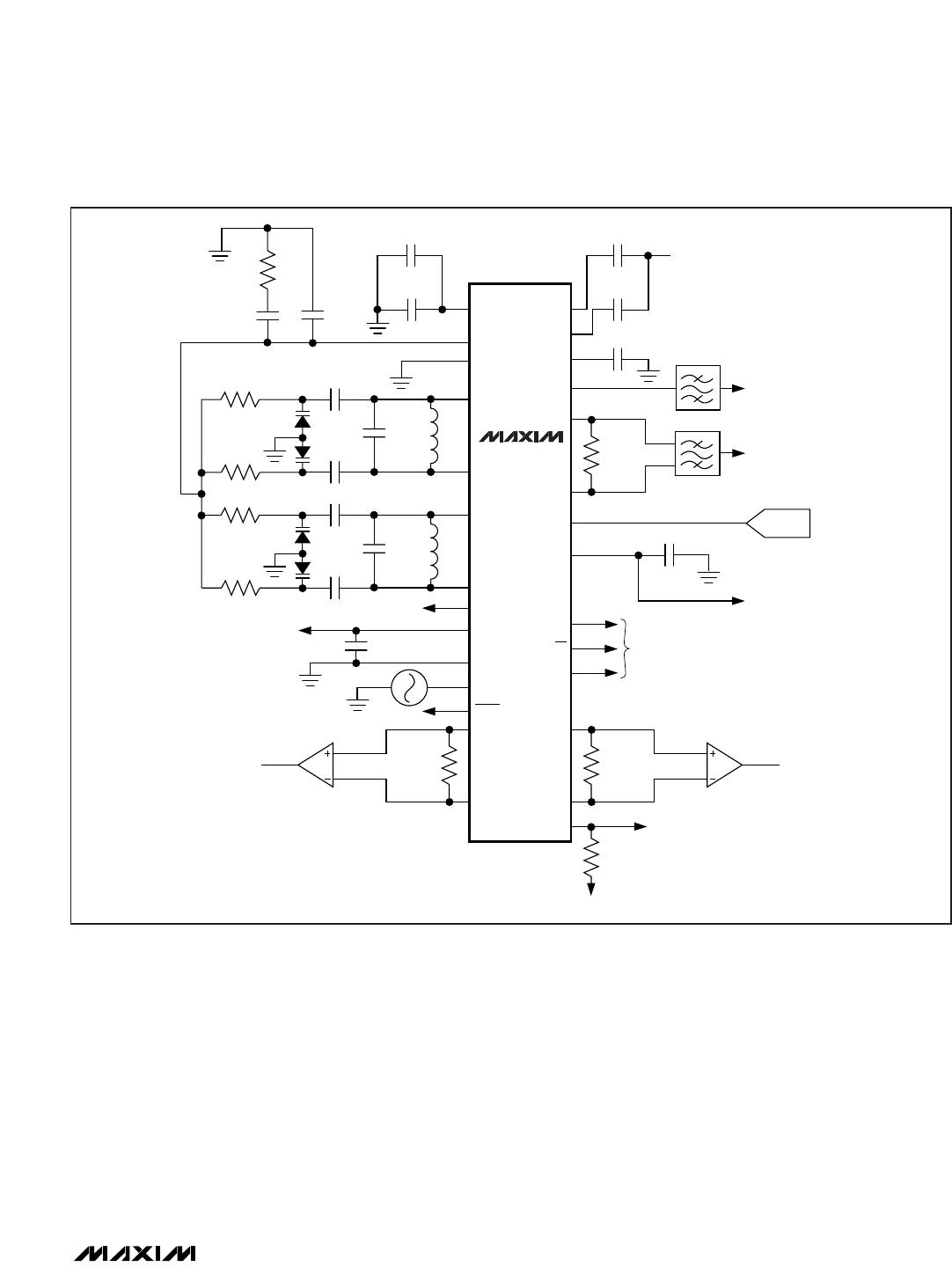
_______________Detailed Description
MAX2306
The MAX2306 is intended for dual-band (PCS and cel-
lular) and dual-mode code division multiple access
(CDMA) and FM applications (Figure 1). The device
includes an IF variable-gain amplifier, quadrature
demodulator, dual VCOs, and dual-frequency synthe-
sizers (Functional Diagram). Dual VCOs are provided
for applications using different IF frequencies for each
mode or band of operation. The analog FM output sig-
nal can be configured for conversion to the I channel,
or it may be converted in quadrature to both the I and
Q channels. The MAX2306’s operation modes are
described in Table 1. These modes are set by pro-
gramming the control register and setting logic levels
on control pins. If MODE is left floating, the internal reg-
ister controls the operation. If driven high or low, mode
will override certain register bits, as shown in Table 1.
MAX2308
The MAX2308 supports dual-band, triple mode with
common IF VCO. As with the MAX2306, the FM mode
can be configured for conversion to the I port or quad-
rature conversion to both the I and Q ports (Figure 2).
The MAX2308’s operational modes are described in
Table 2. These modes are set by programming the con-
trol register.
MAX2309
The MAX2309 quadrature demodulators are simplified
versions of the MAX2306 that can be used in single-
mode CDMA or triple mode using an external FM dis-
criminator (Figure 3). The MAX2309 VCO is optimized
for the 67MHz to 300MHz IF frequency range.
The MAX2309 includes a buffered output for the VCO.
The buffered VCO output can be used to support sys-
tems implementing traditional limiting IF stages for FM
demodulation in dual-mode phones as well as for the
transmit LO in TDD systems. This buffered output can
be configured for the VCO frequency (twice the IF fre-
quency) or one-half the VCO frequency (IF frequency).
The BUFEN pin enables this feature. A standby mode,
in which only the VCO and synthesizer are operational,
can be selected through the serial interface or the
STBY pin. The MAX2309’s operational modes are
described in Table 3. These modes are set by pro-
gramming the control register and/or setting logic levels
on control pins. If the control pins (STBY, BUFEN,
DIVSEL) are left floating, the internal register controls
the operational mode. If driven high or low, the control
pins will override certain register bits, as shown in
Table 3.
Applications Information
Variable-Gain Amplifier and Demodulator
The MAX2306 family provides a VGA with exceptional
gain range. The MAX2306/MAX2308 support multimode
applications with dual differential inputs, selectable with
the IN_SEL (IS) control bit. On the MAX2306, this func-
tion can be controlled with the MODE pin, which over-
rides the IS control bit. The VGA’s gain is controlled
over a 110dB range with the VGC pin. The output of the
VGA drives the RF ports of a quadrature demodulator.
The MAX2306/MAX2308 provide two types of FM
demodulation, controlled by the FM_TYPE (FT) control
bit. When FM_TYPE is “1,” the signal is passed through
both the I and Q signal paths for subsequent lowpass
filtering and A/D conversion at baseband. If FM_TYPE
is “0,” the FM signal is passed through the I mixer only.
Pin Description (continued)
PIN
MAX2306
MAX2308 MAX2309
NAME FUNCTION
25 25 25 BYP
Bypass Node. Must be capacitively decoupled (bypassed)
to ground.
26 26 26 CP_OUT Charge-Pump Output
27 27 27 GND Ground
28 21 N.C. No Connection
28 DIVSEL High selects M1/R1; low selects M2/R2.
Exposed Paddle EP Ground
MAX2306/MAX2308/MAX2309
CDMA IF VGAs and I/Q Demodulators
with VCO and Synthesizer
_______________________________________________________________________________________ 9
Voltage-Controlled Oscillator,
Buffers, and Quadrature Generation
The LO signal for downconversion is provided by a
voltage-controlled oscillator (VCO) consisting of an on-
chip differential oscillator, and an off-chip high-Q reso-
nant network. Figure 4 shows a simplified schematic of
the VCO oscillator. Multiband operation is supported by
the MAX2306 with dual VCOs. VCO_H and VCO_L are
selectable with the MODE pin or the VCO_SEL (VS)
control bit. They oscillate at twice the desired LO fre-
quency. For applications requiring an external LO, the
VCOs can be bypassed with the VCO_BYP (VB) control
bit.
The MAX2309 buffers the output of the VCO and pro-
vides this signal at the LOOUT pin. This signal is
enabled by the BUFEN (BE) control bit or by the
BUFEN control pin. The frequency of this signal is
selected by the BUF_DIV (BD) control bit, and can be
either the VCO frequency or half the VCO frequency.
Quadrature downconversion is realized by providing in-
phase (I) and quadrature-phase (Q) components of the
LO signal to the LO ports of the demodulator described
above. The quadrature LO signals are generated by
dividing the VCO output frequency using two latches.
Figure 1. MAX2306 Typical Operating Circuit
MAX2306
BYP
BYP
FM-
FM+
CDMA+
CDMA
FM
3-WIRE
DAC
0.1µF
0.01µF
0.068µF
47pF
2pF
33pF
0.01µF
10k
2.4k
10k
33pF
47pF
33nH
0.01µF
680
CDMA-
LOCK
VGC
V
CC
V
CC
V
CC
V
CC
DATA
CLK
QOUT+
QOUT-
EN
TANKH-
IOUT-
IOUT+
REF
GND
V
CC
MODE
TANKH+
TANKL-
GND
CP_OUT
BYP
SHDN
TANKL+
0.01µF
V
CC
47pF
10k
47k
Q
10k
2pF
33pF
10k
10k
33pF
I
33nH

MAX2306ETI+

Mfr. #:
Manufacturer:
Maxim Integrated
Description:
Modulator / Demodulator CDMA If VGAs & I/Q Demodulator w/VCO
Lifecycle:
New from this manufacturer.
Delivery:
DHL FedEx Ups TNT EMS
Payment:
T/T Paypal Visa MoneyGram Western Union