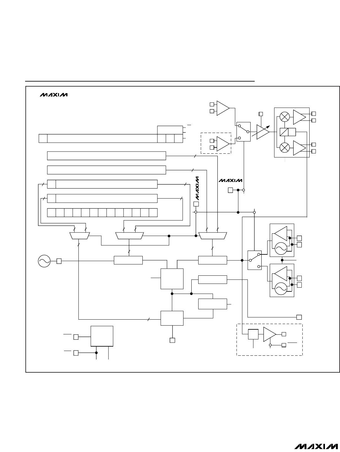
Figure 6. 3-Wire Interface Timing Diagram
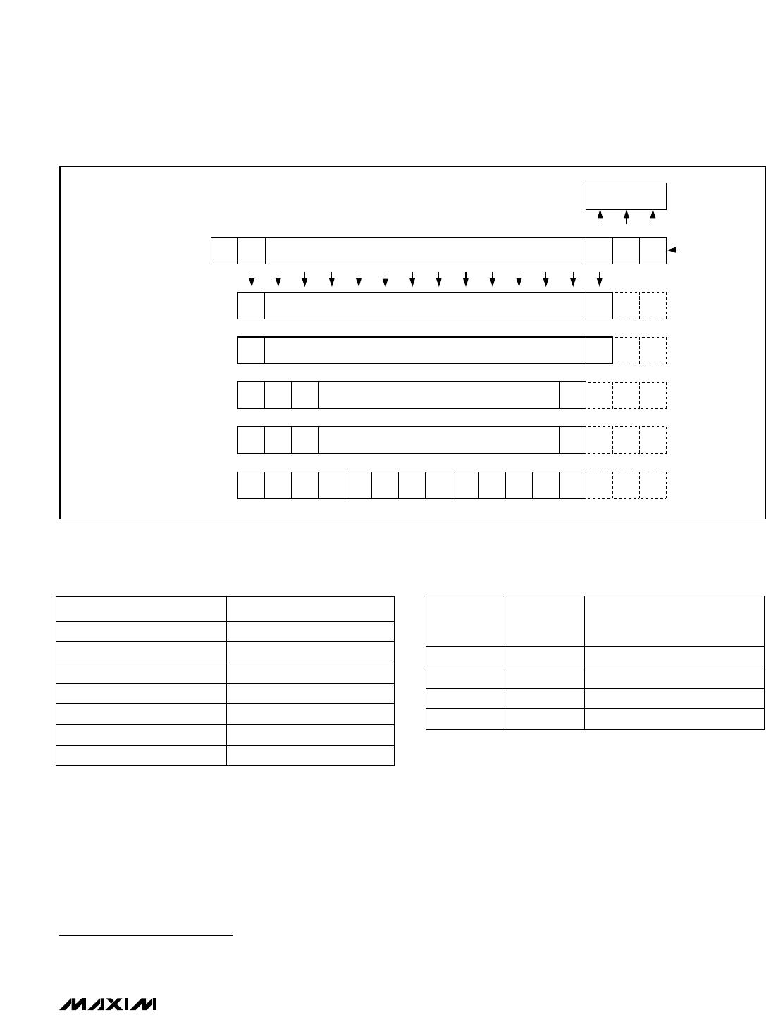
Table 4. Control Register, Default State: 0B57
h,
Address: 110
b
SB
STBY
Logic “0” enables standby mode, which shuts down the VGA and
demodulator stages, leaving the VCO locked and the registers
active.
1
FT FM_TYPE
Active in FM mode. Logic “0” selects quadrature demodulator for
FM mode. Logic “1” selects downconversion to I port.
1
0 3
SD
SHDN
Logic “0” enables register-based shutdown. This mode shuts down
everything except the M and R latches and the serial bus.
1 0
IS IN_SEL Logic “0” selects FM input port. Logic “1” selects CDMA input.1 2
BE
BUFEN
Logic “1” disables LOOUT. Logic “0” enables LOOUT.1 4
VS VCO_SEL Logic “1” selects VCO_H. Logic “0” selects VCO_L.1
DS DIV_SEL Logic “1” selects M1/R1 divide ratios. Logic “0” selects M2/R2.
6
1 8
BD BUF_DIV
Logic “1” selects divide-by-2 on LOOUT port. Logic “0” bypasses
divider.
0 5
VB VCO_BYP Logic “1” bypasses the VCO inputs for external VCO operation.0 7
TE TEST_ENABLE Must be 0 for normal operation.0 10
TC TURBO_CHARGE
Logic “1” activates turbocharge mode, which provides rapid fre-
quency acquisition in the PLL.
1 9
POL CP_POL
Logic “1” causes the charge-pump output CP_OUT to source cur-
rent when f
REF
/R > f
VCO
/M. This state is used when the VCO tune
polarity is such that increasing voltage produces increasing fre-
quency. Logic “0” causes CP_OUT to source current when f
VCO
/M
> f
REF
/R. This state is used when increasing tune voltage causes
the VCO frequency to decrease.
1 11
BIT NAME FUNCTIONBIT ID
TM TEST_MODE Must be 0 for normal operation.0 12
BIT
LOCATION
0 = LSB
POWER-
UP
STATE