PIN CONFIGURATIONS
a
Rail-to-Rail High Output
Current Operational Amplifiers
OP179/OP279
GENERAL DESCRIPTION
The OP179 and OP279 are rail-to-rail, high output current,
single-supply amplifiers. They are designed for low voltage
applications that require either current or capacitive load drive
capability. The OP179/OP279 can sink and source currents of
±60 mA (typical) and are stable with capacitive loads to 10 nF.
Applications that benefit from the high output current of the
OP179/OP279 include driving headphones, displays, transform-
ers and power transistors. The powerful output is combined with a
unique input stage that maintains very low distortion with wide
common-mode range, even in single supply designs.
The OP179/OP279 can be used as a buffer to provide much
greater drive capability than can usually be provided by CMOS
outputs. CMOS ASICs and DAC often have outputs that can
swing to both the positive supply and ground, but cannot drive
more than a few milliamps.
Bandwidth is typically 5 MHz and the slew rate is 3 V/µs, making
these amplifiers well suited for single supply applications that
require audio bandwidths when used in high gain configurations.
Operation is guaranteed from voltages as low as 4.5 V, up to 12 V.
Very good audio performance can be attained when using the
OP179/OP279 in 5 volt systems. THD is below 0.01% with a
600 Ω load, and noise is a respectable 21 nV/√Hz. Supply current
is less than 3.5 mA per amplifier.
The single OP179 is available in the 5-lead SOT-23-5 package.
It is specified over the industrial (–40°C to +85°C) tempera-
ture range.
The OP279 is available in 8-lead TSSOP and SO-8 surface
mount packages. They are specified over the industrial (–40°C
to +85°C) temperature range.
8-Lead SOIC and TSSOP
SO-8 (S) and RU-8
1
2
3
4
8
7
6
5
OP279
ⴚIN A
Vⴚ
+IN A
OUT B
ⴚIN B
V+
+IN B
OUT A
FEATURES
Rail-to-Rail Inputs and Outputs
High Output Current: ⴞ60 mA
Single Supply: 5 V to 12 V
Wide Bandwidth: 5 MHz
High Slew Rate: 3 V/s
Low Distortion: 0.01%
Unity-Gain Stable
No Phase Reversal
Short-Circuit Protected
Drives Capacitive Loads: 10 nF
APPLICATIONS
Multimedia
Telecom
DAA Transformer Driver
LCD Driver
Low Voltage Servo Control
Modems
FET Drivers
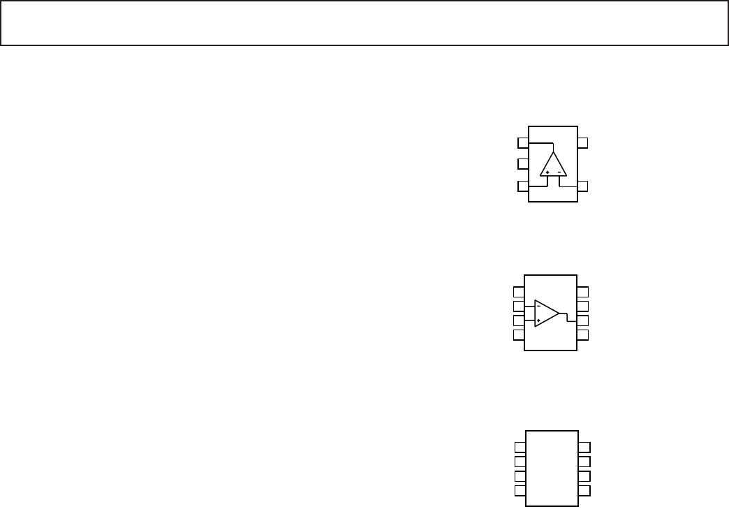
5-Lead SOT-23-5
(RT-5)
1
2
3
5
4
ⴚIN A
+IN A
V–
OUT A
OP179
V+
8-Lead SOIC
(S Suffix)
1
2
3
4
8
7
6
5
OP179
ⴚIN A
Vⴚ
+IN A
V+
OUT A
NC
NC
NC
NC = NO CONNECT
REV. G
Information furnished by Analog Devices is believed to be accurate and
reliable. However, no responsibility is assumed by Analog Devices for its
use, nor for any infringements of patents or other rights of third parties that
may result from its use. No license is granted by implication or otherwise
under any patent or patent rights of Analog Devices.
One Technology Way, P.O. Box 9106, Norwood, MA 02062-9106, U.S.A.
Tel: 781/329-4700 www.analog.com
Fax: 781/326-8703 © Analog Devices, Inc., 2002