OP179/OP279
–7–
REV. G
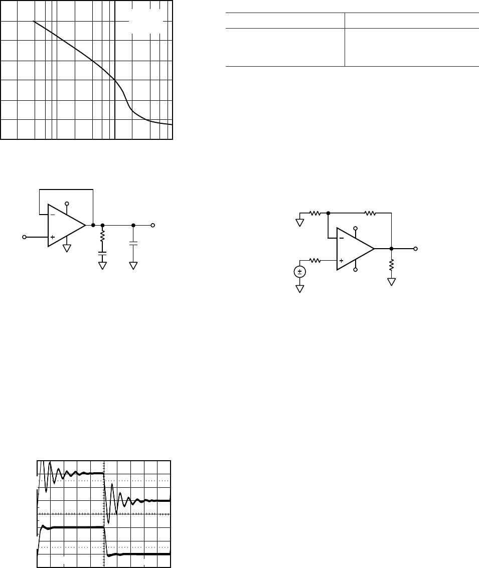
In order to achieve rail-to-rail output behavior, the OP179/OP279
design employs a complementary common-emitter (or g
m
R
L
)
output stage (Q15-Q16), as illustrated in Figure 2. These
amplifiers provide output current until they are forced into
saturation, which occurs at approximately 50 mV from either
supply rail. Thus, their saturation voltage is the limit on the
maximum output voltage swing in the OP179/OP279. The
output stage also exhibits voltage gain, by virtue of the use of
common-emitter amplifiers; and, as a result, the voltage gain of
the output stage (thus, the open-loop gain of the device) exhib-
its a strong dependence to the total load resistance at the output
of the OP179/OP279 as illustrated in TPC 7.
Q7
Q3
Q15
Q9
105
V
POS
V
NEG
Q13
V
OUT
Q4
Q16
I3
I4
Q11
Q12
Q5
Q10
I2
Q1
Q2
I1
Q8
Q6
105
Q14
150
Figure 2. OP179/OP279 Equivalent Output Circuit
Input Overvoltage Protection
As with any semiconductor device, whenever the condition
exists for the input to exceed either supply voltage, the device’s
input overvoltage characteristic must be considered. When an
overvoltage occurs, the amplifier could be damaged, depending
on the magnitude of the applied voltage and the magnitude of
the fault current. Figure 3 illustrates the input overvoltage char-
acteristic of the OP179/OP279. This graph was generated with
the power supplies at ground and a curve tracer connected to
the input. As can be seen, when the input voltage exceeds either
supply by more than 0.6 V, internal pn-junctions energize,
which allows current to flow from the input to the supplies. As
illustrated in the simplified equivalent input circuit (Figure 1),
the OP179/OP279 does not have any internal current limiting
resistors, so fault currents can quickly rise to damaging levels.
This input current is not inherently damaging to the device as
long as it is limited to 5 mA or less. For the OP179/OP279, once
the input voltage exceeds the supply by more than 0.6 V, the
input current quickly exceeds 5 mA. If this condition continues to
exist, an external series resistor should be added. The size of the
resistor is calculated by dividing the maximum overvoltage by
5 mA. For example, if the input voltage could reach 100 V, the
external resistor should be (100 V/5 mA) = 20 k. This resis-
tance should be placed in series with either or both inputs if they
are exposed to an overvoltage. Again, in order to ensure optimum
dc and ac performance, it is important to balance source imped-
ance levels. For more information on general overvoltage charac-
teristics of amplifiers refer to the 1993 Seminar Applications Guide,
available from the Analog Devices Literature Center.
5
3
5
2.0
4
1
2
1
2
3
4
2.01.001.0
0
INPUT CURRENT mA
INPUT VOLTAGE V
Figure 3. OP179/OP279 Input Overvoltage Characteristic
Output Phase Reversal
Some operational amplifiers designed for single-supply operation
exhibit an output voltage phase reversal when their inputs are
driven beyond their useful common-mode range. Typically for
single-supply bipolar op amps, the negative supply determines
the lower limit of their common-mode range. With these devices,
external clamping diodes, with the anode connected to ground
and the cathode to the inputs, input signal excursions are pre-
vented from exceeding the device’s negative supply (i.e., GND),
preventing a condition that could cause the output voltage to
change phase. JFET input amplifiers may also exhibit phase
reversal and, if so, a series input resistor is usually required to
prevent it.
The OP179/OP279 is free from reasonable input voltage range
restrictions provided that input voltages no greater than the
supply voltages are applied. Although the device’s output will
not change phase, large currents can flow through the input
protection diodes, shown in Figure 1. Therefore, the technique
recommended in the Input Overvoltage Protection section should
be applied in those applications where the likelihood of input
voltages exceeding the supply voltages is possible.
Capacitive Load Drive
The OP179/OP279 has excellent capacitive load driving capa-
bilities. It can drive up to 10 nF directly as the performance
graph titled Small Signal Overshoot vs. Load Capacitance
(TPC 18) shows. However, even though the device is stable, a
capacitive load does not come without a penalty in bandwidth.
As shown in Figure 4, the bandwidth is reduced to under 1 MHz
for loads greater than 3 nF. A “snubber” network on the output
will not increase the bandwidth, but it does significantly reduce
the amount of overshoot for a given capacitive load. A snubber
consists of a series R-C network (R
S
, C
S
), as shown in Figure 5,
connected from the output of the device to ground. This net-
work operates in parallel with the load capacitor, C
L
, to provide
phase lag compensation. The actual value of the resistor and
capacitor is best determined empirically.
OP179/OP279
–8–
REV. G
7
2
0
0.01 0.100 101
5
1
3
4
6
CAPACITIVE LOAD nF
BANDWIDTH MHz
V
S
5V
R
L
1k
T
A
25C
Figure 4. OP179/OP279 Bandwidth vs. Capacitive Load
1/2
OP279
R
S
20V
C
S
1F
C
L
10nF
5V
V
IN
100mV p-p
V
OUT
Figure 5. Snubber Network Compensates for Capacitive
Load
The first step is to determine the value of the resistor, R
S
. A
good starting value is 100 (typically, the optimum value will
be less than 100 ). This value is reduced until the small-signal
transient response is optimized. Next, C
S
is determined—10 µF
is a good starting point. This value is reduced to the smallest
value for acceptable performance (typically, 1 µF). For the case
of a 10 nF load capacitor on the OP179/OP279, the optimal
snubber network is a 20 in series with 1 µF. The benefit is
immediately apparent as seen in the scope photo in Figure 6.
The top trace was taken with a 10 nF load and the bottom trace
with the 20 , 1 µF snubber network in place. The amount of
overshot and ringing is dramatically reduced. Table I illustrates a
few sample snubber networks for large load capacitors.
90
100
10nF LOAD
ONLY
SNUBBER
IN CIRCUIT
10
0%
50mV
2s
Figure 6. Overshoot and Ringing Are Reduced by Adding
a “Snubber” Network in Parallel with the 10 nF Load
Table I. Snubber Networks for Large Capacitive Loads
Load Capacitance (C
L
) Snubber Network (R
S
, C
S
)
10 nF 20 , 1 µF
100 nF 5 , 10 µF
1 µF0 , 10 µF
Overload Recovery Time
Overload, or overdrive, recovery time of an operational amplifier
is the time required for the output voltage to recover to its linear
region from a saturated condition. This recovery time is impor-
tant in applications where the amplifier must recover after a
large transient event. The circuit in Figure 7 was used to
evaluate the OP179/OP279’s overload recovery time. The
OP179/OP279 takes approximately 1 µs to recover from positive
saturation and approximately 1.2 µs to recover from negative
saturation.
1/2
OP279
R
L
499
+5V
V
OUT
5V
R3
10k
R2
1k
R1
909
2V p-p
@ 100Hz
Figure 7. Overload Recovery Time Test Circuit
Output Transient Current Recovery
In many applications, operational amplifiers are used to provide
moderate levels of output current to drive the inputs of ADCs,
small motors, transmission lines and current sources. It is in these
applications that operational amplifiers must recover quickly to
step changes in the load current while maintaining steady-state
load current levels. Because of its high output current capability
and low closed-loop output impedance, the OP179/OP279 is an
excellent choice for these types of applications. For example,
when sourcing or sinking a 25 mA steady-state load current, the
OP179/OP279 exhibits a recovery time of less than 500 ns to
0.1% for a 10 mA (i.e., 25 mA to 35 mA and 35 mA to 25 mA)
step change in load current.
A Precision Negative Voltage Reference
In many data acquisition applications, the need for a precision
negative reference is required. In general, any positive voltage
reference can be converted into a negative voltage reference
through the use of an operational amplifier and a pair of matched
resistors in an inverting configuration. The disadvantage to that
approach is that the largest single source of error in the circuit is
the relative matching of the resistors used.
The circuit illustrated in Figure 8 avoids the need for tightly
matched resistors with the use of an active integrator circuit. In
this circuit, the output of the voltage reference provides the
input drive for the integrator. The integrator, to maintain circuit
equilibrium, adjusts its output to establish the proper relation-
ship between the reference’s V
OUT
and GND. Thus, various
negative output voltages can be chosen simply by substituting
for the appropriate reference IC (see table). To speed up the
OP179/OP279
–9–
REV. G
ON-OFF settling time of the circuit, R2 can be reduced to
50 k or less. Although the integrator’s time constant chosen
here is 1 ms, room exists to trade off circuit bandwidth and
noise by increasing R3 and decreasing C2. The SHUTDOWN
feature is maintained in the circuit with the simple addition of a
PNP transistor and a 10 k resistor. One caveat with this
approach should be mentioned: although rail-to-rail output
amplifiers work best in the application, these operational ampli-
fiers require a finite amount (mV) of headroom when required
to provide any load current. The choice for the circuit’s negative
supply should take this issue into account.
R4
10
1/2
OP279
+5V
10V
R3
1k
C2
1F
C1
1F
R2
100k
U1
REF195
GND
R5
10k
R1
10k
2N3904
4
6
2
3
SHUTDOWN
TTL/CMOS
+5V
V
REF
U1
REF192
REF193
REF196
REF194
V
OUT
(V)
2.5
3.0
3.3
4.5
Figure 8. A Negative Precision Voltage Reference That
Uses No Precision Resistors Exhibits High Output Current
Drive
A High Output Current, Buffered Reference/Regulator
Many applications require stable voltage outputs relatively close
in potential to an unregulated input source. This “low dropout”
type of reference/regulator is readily implemented with a rail-to-
rail output op amp, and is particularly useful when using a
higher current device such as the OP179/OP279. A typical
example is the 3.3 V or 4.5 V reference voltage developed from
a 5 V system source. Generating these voltages requires a three-
terminal reference, such as the REF196 (3.3 V) or the REF194
(4.5 V), both of which feature low power, with sourcing outputs
of 30 mA or less. Figure 9 shows how such a reference can be
outfitted with an OP179/OP279 buffer for higher currents and/
or voltage levels, plus sink and source load capability.
C2
0.1F
R2
10k
1%
U2
1/2 OP279
V
OUT1
=
3.3V @ 30mA
R5
1
C5
10F/25V
TANTALUM
R1
10k
1%
C1
0.1F
V
S
5V
V
OUT2
=
3.3V
C4
1F
6
2
3
4
V
OUT
COMMON
C3
0.1F
V
C
ON/OFF
CONTROL
INPUT CMOS HI
(OR OPEN) = ON
LO = OFF
V
S
COMMON
R3
(SEE TEXT)
R4
3.3k
U1
REF196
Figure 9. A High Output Current Reference/Regulator
The low dropout performance of this circuit is provided by stage
U2, one-half of an OP179/OP279 connected as a follower/buffer
for the basic reference voltage produced by U1. The low voltage
saturation characteristic of the OP179/OP279 allows up to 30 mA
of load current in the illustrated use, as a 5 V to 3.3 V converter
with high dc accuracy. In fact, the dc output voltage change for
a 30 mA load current delta measures less than 1 mV. This
corresponds to an equivalent output impedance of < 0.03 . In
this application, the stable 3.3 V from U1 is applied to U2
through a noise filter, R1-C1. U2 replicates the U1 voltage
within a few mV, but at a higher current output at V
OUT1
, with
the ability to both sink and source output current(s)—unlike
most IC references. R2 and C2 in the feedback path of U2
provide bias compensation for lowest dc error and additional
noise filtering.
Transient performance of the reference/regulator for a 10 mA
step change in load current is also quite good and is determined
largely by the R5-C5 output network. With values as shown, the
transient is about 10 mV peak and settles to within 2 mV in 8 µs,
for either polarity. Although room exists for optimizing the
transient response, any changes to the R5-C5 network should
be verified by experiment to preclude the possibility of excessive
ringing with some capacitor types.
To scale V
OUT2
to another (higher) output level, the optional
resistor R3 (shown dotted) is added, causing the new V
OUT1
to
become:
VV
R
R
OUT1 OUT2
+
1
2
3
As an example, for a V
OUT1
= 4.5 V, and V
OUT2
= 2.5 V from a
REF192, the gain required of U2 is 1.8 times, so R2 and R3
would be chosen for a ratio of 0.8:1, or 18 k:22.5 k. Note that
for the lowest V
OUT1
dc error, the parallel combination of R2 and
R3 should be maintained equal to R1 (as here), and the R2-R3
resistors should be stable, close tolerance metal film types.
The circuit can be used as shown as either a 5 V to 3.3 V reference/
regulator, or it can be used with ON/OFF control. By driving
Pin 3 of U1 with a logic control signal as noted, the output is
switched ON/OFF. Note that when ON/OFF control is used,
resistor R4 should be used with U1 to speed ON-OFF switching.
Direct Access Arrangement for Telephone Line Interface
Figure 10 illustrates a 5 V only transmit/receive telephone line
interface for 110 transmission systems. It allows full duplex
transmission of signals on a transformer coupled 110 line in
a differential manner. Amplifier A1 provides gain that can be
adjusted to meet the modem output drive requirements. Both
A1 and A2 are configured to apply the largest possible signal on a
single supply to the transformer. Because of the OP179/OP279’s
high output current drive and low dropout voltage, the largest
signal available on a single 5 V supply is approximately 4.5 V p-p
into a 110 transmission system. Amplifier A3 is configured as
a difference amplifier to extract the receive signal from the
transmission line for amplification by A4. A4’s gain can be adjusted
in the same manner as A1’s to meet the modem’s input signal
requirements. Standard resistor values permit the use of SIP
(Single In-line Package) format resistor arrays. Couple this with
the OP179/OP279’s 8-lead SOIC footprint and this circuit
offers a compact, cost-sensitive solution.

OP279GSZ

Mfr. #:
Manufacturer:
Analog Devices Inc.
Description:
Operational Amplifiers - Op Amps RR Hi-Output Current
Lifecycle:
New from this manufacturer.
Delivery:
DHL FedEx Ups TNT EMS
Payment:
T/T Paypal Visa MoneyGram Western Union