OP179/OP279
–10–
REV. G
6.2V
6.2V
TRANSMIT
TXA
RECEIVE
RXA
C1
0.1F
R1
10k
R2
9.09k
2k
P1
TX GAIN
ADJUST
A1
A2
A3
A4
A1, A2 = 1/2 OP279
A3, A4 = 1/2 OP279
R3
55
R4
55
1:1
T1
TO TELEPHONE
LINE
1
2
3
7
6
5
2
3
1
6
5
7
10F
R7
10k
R8
10k
R5
10k
R6
10k
R9
10k
R14
9.09k
R10
10k
R11
10k
R12
10k
R13
10k
C2
0.1F
P2
RX GAIN
ADJUST
2k
Z
O
110
5V DC
Figure 10. A Single-Supply Direct Access Arrangement for
Modems
A Single-Supply, Remote Strain Gage Signal Conditioner
The circuit in Figure 11 illustrates a way by which the OP179/
OP279 can be used in a 12 V single supply, 350 strain gage
signal conditioning circuit. In this circuit, the OP179/OP279
serves two functions: (1) By servoing the output of the REF43’s
2.5 V output across R1, it provides a 20 mA drive to the 350
strain gage. In this way, small changes in the strain gage pro-
duce large differential output voltages across the AMP04’s
inputs. (2) To maximize the circuit’s dynamic range, the other
half of the OP179/OP279 is configured as a supply-splitter
connected to the AMP04’s REF terminal. Thus, tension or
compression in the application can be measured by the circuit.
REF43
AMP04
0.1F
2
6
4
2.5V
3
1
8
4
2
A1
7
1
8
6
3
2
4
C
X
C2
0.1F
R4
1k
12V
5
V
O
80mV/
V
O
COMMON
R1
124
0.1%, LOW TCR
100-ft TWISTED PAIR
BELDEN TYPE 9502
S+
S
350
STRAIN GAGE
F
F+
A2
12V
R2
10k
R3
10k
C1
10F
7
6
5
+6V
A1, A2 = 1/2 OP279
12V
20mA DRIVE
Figure 11. A Single-Supply, Remote Strain Gage Signal
Conditioner
The AMP04 is configured for a gain of 100, producing a circuit
sensitivity of 80 mV/. Capacitor C2 is used across the AMP04’s
Pins 8 and 6 to provide a 16-Hz noise filter. If additional noise
filtering is required, an optional capacitor, C
X
, can be used across
the AMP04’s input to provide differential-mode noise rejection.
A Single-Supply, Balanced Line Driver
The circuit in Figure 12 is a unique line driver circuit topology
used in professional audio applications and has been modified
for automotive audio applications. On a single 12 V supply, the
line driver exhibits less than 0.02% distortion into a 600 load
across the entire audio band (not shown). For loads greater than
600 , distortion performance improves to where the circuit
exhibits less than 0.002%. The design is a transformerless, balanced
transmission system where output common-mode rejection of
noise is of paramount importance. Like the transformer-based
system, either output can be shorted to ground for unbalanced
line driver applications without changing the circuit gain of 1.
Other circuit gains can be set according to the equation in the
diagram. This allows the design to be easily configured for
noninverting, inverting, or differential operation.
R
L
600
C1
22F
A2
7
6
5
3
1
2
A1
12V
R1
10k
R2
10k
R11
10k
R7
10k
6
7
5
A1
12V
12V
R8
100k
R9
100k
C2
1F
R12
10k
R14
50
A2
1
2
3
R3
10k
R6
10k
R13
10k
C3
47F
V
O1
V
O2
C4
47F
A1, A2 = 1/2 OP279
GAIN =
R3
R2
SET: R7, R10, R11 = R2
SET: R6, R12, R13 = R3
V
IN
R5
50
Figure 12. A Single-Supply, Balanced Line Driver for
Automotive Applications
OP179/OP279
–11–
REV. G
UNITY-GAIN, SALLEN-KEY (VCVS) FILTERS
High Pass Configurations
Figure 14a is the HP form of a unity-gain 2-pole SK filter
using an OP179/OP279 section. For this filter and its LP coun-
terpart, the gain in the passband is inherently unity, and the
signal phase is noninverting due to the follower hookup. For
simplicity and practicality, capacitors C1-C2
are set equal, and
resistors R2-R1
are adjusted to a ratio “N,” which provides the
filter damping “α” as per the design expressions. An HP design
starts with the selection of standard capacitor values for C1 and
C2, and a calculation of N. R1 and R2 are then calculated as
per the figure expressions.
In these examples, α (or 1/Q) is set equal to 2, providing a
Butterworth (maximally flat) response characteristic. The filter
corner frequency is normalized to 1 kHz, with resistor values
shown in both rounded and (exact) form. Various other two-pole
response shapes are also possible with appropriate selection of
α. For a given response type (α), frequency can be easily scaled,
using proportional R or C values.
+V
S
V
S
U1A
OP279
1
3
2
4
8
IN
R2
22k
(22.508k)
R1
11k
(11.254k)
C2
0.01F
R = R2
0.1F
Z
f
(HIGH PASS)
C1
0.01F
GIVEN: ALPHA, F
SET C1 = C2 = C
ALPHA = 2/(N^0.5) = 1/Q
N = 4/(ALPHA)^2 = R2/R1
R1 = 1/(2
*
PI
*
F
*
C
*
(N^0.5))
R2 = N
*
R1
1kHz BW SHOWN
OUT
7
5
6
R = R1+R2
Z
f
(LOW PASS)
GIVEN: ALPHA, F
SET R1 = R2 = R
ALPHA = 2/(M^0.5) = 1/Q
N = 4/(ALPHA)^2 = C2/C1
PICK C1
C1 = M*C1
R = 1/(2*P1*F*C1* (M^0.5))
1kHz BW SHOWN
IN
R2
11k
(11.254k)
C2
0.01F
0.1F
C1
0.02F
OUT
U1B
OP279
R1
11k
(11.254k)
a. High Pass
b. Low Pass
Figure 14. Two-Pole Unity-Gain Sallen Key HP/LP Filters
Low Pass Configurations
In the LP SK arrangement of Figure 14b, R and C elements are
interchanged, and the resistors are made equal. Here the C2/C1
ratio “M” is used to set the filter α, as noted. This design is begun
with the choice of a standard capacitor value for C1 and a calcu-
lation of M, which forces a value of “M × C1” for C2. Then, the
value “R” for R1 and R2 is calculated as per the expression.
For highest performance, the passive components used for tun-
ing active filters deserve attention. Resistors should be 1%, low
TC, metal film types of the RN55 or RN60 style, or similar.
A Single-Supply Headphone Amplifier
Because of its high speed and large output drive, the OP179/P279
makes for an excellent headphone driver, as illustrated in Figure
13. Its low supply operation and rail-to-rail inputs and outputs
give a maximum signal swing on a single 5 V supply. To ensure
maximum signal swing available to drive the headphone, the
amplifier inputs are biased to V+/2, which is in this case 2.5 V.
The 100 k resistor to the positive supply is equally split into
two 50 k with their common point bypassed by 10 µF to pre-
vent power supply noise from contaminating the audio signal.
16
50k
220F
LEFT
HEADPHONE
10F
50k
50k
100k
10F
LEFT
INPUT
+V + 5V
1/2
OP279
16
50k
220F
RIGHT
HEADPHONE
10F
50k
50k
100k
10F
RIGHT
INPUT
+V
+V + 5V
1/2
OP279
Figure 13. A Single-Supply, Stereo Headphone Driver
The audio signal is then ac-coupled to each input through a
10 µF capacitor. A large value is needed to ensure that the
20 Hz audio information is not blocked. If the input already has
the proper dc bias, the ac coupling and biasing resistors are not
required. A 220 µF capacitor is used at the output to couple the
amplifier to the headphone. This value is much larger than that
used for the input because of the low impedance of the head-
phones, which can range from 32 to 600 . An additional
16 resistor is used in series with the output capacitor to pro-
tect the op amp’s output stage by limiting capacitor discharge
current. When driving a 48 load, the circuit exhibits less than
0.02% THD+N at low output drive levels (not shown). The
OP179/OP279’s high current output stage can drive this heavy
load to 4 V p-p and maintain less than 1% THD+N.
Active Filters
Several active filter topologies are useful with the OP179/OP279.
Among these are two popular architectures, the familiar Sallen-
Key (SK) voltage controlled voltage source (VCVS) and the
multiple feedback (MFB) topologies. These filter types can be
arranged for high pass (HP), low pass (LP), and band-pass (BP)
filters. The SK filter type uses the op amp as a fixed gain voltage
follower at unity or a higher gain, while the MFB structure uses
it as an inverting stage. Discussed here are simplified, 2-pole
forms of these filters, highly useful as system building blocks.
OP179/OP279
–12–
REV. G
loading can be tempered somewhat by using a small series input
resistance of about 100 , but can still be an issue.
7
6
5
0.1F
GIVEN:
ALPHA, F AND H (PASSBAND GAIN)
ALPHA = 1/Q
PICK A STD C1 VALUE, THEN:
C3 = C1, C2 = C1/H
R1 = ALPHA/((2
*
PI
*
F
*
C1)
*
(2+(1/H)))
R2 = (H
*
(2+(1/H)))/(ALPHA
*
(2
*
PI
*
F
*
C1))
1kHz BW EXAMPLE SHOWN
(NOTE: SEE TEXT ON C1 LOADING
CONSIDERATIONS)
IN
R1
7.5k
OUT
U1B
OP279
R2
33.6k
C3
0.01F
C2
0.01F
C1
0.01F
Z
b
R = R2
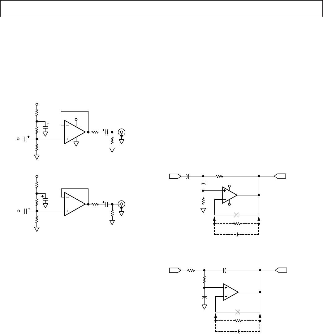
Figure 15. Two-Pole, High Pass Multiple Feedback Filters
In this example, the filter gain is set to unity, the corner fre-
quency is 1 kHz, and the response is a Butterworth type. For
applications where dc output offset is critical, bias current com-
pensation can be used for the amplifier. This is provided by
network Z
b
, where R is equal to R2, and the capacitor provides
a noise bypass.
Low Pass Configurations
Figure 16 is a LP MFB 2-pole filter using an OP179/OP279
section. For this filter, the gain in the pass band is user con-
figurable over a wide range, and the pass band signal phase is
inverting. Given the design parameters for α, F, and H, a simplified
design process is begun by picking a standard value for C2. Then
C1
and resistors R1-R3
are selected as per the relationships
noted. Optional dc bias current compensation is provided by Z
b
,
where R is equal to the value of R3 plus the parallel equivalent
value of R1
and R2.
7
5
6
(R1 R2)+R3
GIVEN:
ALPHA, F AND H (PASSBAND GAIN)
ALPHA = 1/Q
PICK A STD C2 VALUE, THEN:
C1 = C2 (4 (H +1))/ALPHA^2
R1 = ALPHA/(4 H PI F C2)
R2 = H R1
R3 = ALPHA/(4 (H + 1) PI F C2)
1kHz BW EXAMPLE SHOWN
(NOTE: SEE TEXT ON C1 LOADING
CONSIDERATIONS)
IN
OUT
U1B
OP279
R1
11.3k
R2
11.3k
R3
5.62k
C2
0.01F
0.1F
Z
b
C1
0.04F
Figure 16. Two-Pole, Low-Pass Multiple Feedback Filters
Gain of this filter, H, is set here by resistors R2 and R1 (as in a
standard op amp inverter), and can be just as precise as these
resistors allow at low frequencies. Because of this flexible and
accurate gain characteristic, plus a low range of component
value spread, this filter is perhaps the most practical of all the
MFB types. Capacitor ratios are best satisfied by paralleling two
or more common types, as in the example, which is a 1 kHz
unity-gain Butterworth filter.
Capacitors should be 1% or 2% film types preferably, such as
polypropylene or polystyrene, or NPO (COG) ceramic for
smaller values. Somewhat lesser performance is available with
the use of polyester capacitors.
Parasitic Effects in Sallen-Key Implementations
In designing these circuits, moderately low (10 k or less) val-
ues for R1-R2 can be used to minimize the effects of Johnson
noise when critical, with, of course, practical tradeoffs of capaci-
tor size and expense. DC errors will result for larger values of
resistance, unless bias current compensation is used. To add
bias compensation in the HP filter of Figure 14a, a feedback
compensation resistor with a value equal to R2 is used, shown
optionally as Z
f
. This will minimize bias induced offset, reduc-
ing it to the product of the OP179/OP279’s I
OS
and R2. Similar
compensation is applied to the LP filter, using a Z
f
resistance of
R1 + R2. Using dc compensation and relatively low filter values,
filter output dc errors using the OP179/OP279 will be domi-
nated by V
OS
, which is limited to 4 mV or less. A caveat here is
that the additional resistors increase noise substantially—for
example, an unbypassed 10 k resistor generates 12 nV/Hz
of noise. However, the resistance can be ac-bypassed to elimi-
nate noise with a simple shunt capacitor, such as 0.1 µF.
Sallen-Key Implementations in Single-Supply Applications
The hookups shown illustrate a classical dual supply op amp
application, which for the OP179/OP279 would use supplies up
to ±5 V. However, these filters can also use the op amp in a
single-supply mode, with little if any alteration to the filter itself.
To operate single supply, the OP179/OP279 is powered from
5 V at Pin 8 with Pin 4 grounded. The input dc bias for the op
amp must be supplied from a dc source equal to one-half supply,
or 2.5 V in this case.
For the HP section, dc bias is applied to the common end of R2.
R2 is simply returned to an ac ground that is a well-bypassed
2:1 divider across the 5 V source. This can be as simple as a pair
of 100 k resistors with a 10 µF bypass cap. The output from
the stage is then ac coupled, using an appropriate coupling cap
from U1A to the next stage. For the LP section dc bias is applied
to the input end of R1, in common with the input signal. This
dc can be taken from an unbypassed dual 100 k divider across
the supply, with the input signal ac coupled to the divider and R1.
Multiple Feedback Filters
MFB filters, like their SK relatives, can be used as building
blocks as well. They feature LP and HP operation as well, but
can also be used in a band-pass BP mode. They have the property
of inverting operation in the pass band, since they are based on
an inverting amplifier structure. Another useful asset is their
ability to be easily configured for gain.
High Pass Configurations
Figure 15 shows an HP MFB 2-pole filter using an OP179/
OP279 section. For this filter, the gain in the pass band is user
configurable, and the signal phase is inverting. The circuit uses
one more tuning component than the SK types. For simplicity,
capacitors C1 and C3
are set to equal standard values, and resis-
tors R1-R2
are selected as per the relationships noted. Gain of
this filter, H, is set by capacitors C1 and C2, and this factor
limits both gain selectability and precision. Also, input capaci-
tance C1 makes the load seen by the driving stage highly reactive,
and limits overall practicality of this filter. The dire effect of C1

OP279GSZ

Mfr. #:
Manufacturer:
Analog Devices Inc.
Description:
Operational Amplifiers - Op Amps RR Hi-Output Current
Lifecycle:
New from this manufacturer.
Delivery:
DHL FedEx Ups TNT EMS
Payment:
T/T Paypal Visa MoneyGram Western Union