OP179/OP279
–13–
REV. G
V
IN
3
2
1
U1A
OP279
+V
S
4
–V
S
R1
31.6k⍀
C1
0.01F
C2
0.01F
R2
31.6k⍀
R5
31.6k⍀
R6
31.6k⍀
R4
49.9⍀
HI
LO
500Hz AND UP
DC – 500Hz
6
5
7
C3
0.01F
U1B
OP279
C4
0.02F
R7
15.8k⍀
R3
49.9⍀
0.1F
0.1F
100F/25V
100F/25V
+V
S
–V
S
TO U1
+5V
–5V
COM
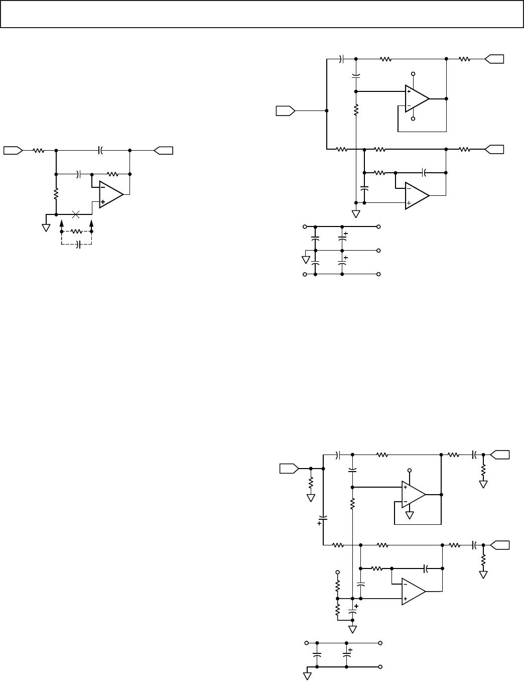
Figure 18. Two-Way Active Crossover Networks
In the filter sections, component values have been selected for
good balance between reasonable physical/electrical size, and
lowest noise and distortion. DC offset errors can be minimized
by using dc compensation in the feedback and bias paths, ac
bypassed with capacitors for low noise. Also, since the network
input is reactive, it should driven from a directly coupled low
impedance source at V
IN
.
Figure 19 shows this filter architecture adapted for single-supply
operation from a 5 V dc source, along the lines discussed
previously.
V
IN
3
2
1
U1A
OP279
+V
S
4
R1
31.6k⍀
C1
0.01F
C2
0.01F
R2
31.6k⍀
R5
31.6k⍀
R6
31.6k⍀
R4
49.9⍀
HI
LO
500Hz
AND UP
DC –
500Hz
6
5
7
C3
0.01F
U1B
OP279
C4
0.02F
R7
15.8k⍀
R3
49.9⍀
10F
10F
100k⍀
+V
S
10F
100k⍀
100k⍀
C
IN
10F
R
IN
100k⍀
0.1F 100F/25V
+V
S
TO U1
+5V
COM
+
100k⍀
+
Figure 19. A Single-Supply, Two-Way Active Crossover
Band-pass Configurations
The MFB band-pass filter using an OP179/OP279 section is
shown in Figure 17. This filter provides reasonably stable medium
Q designs for frequencies of up to a few kHz. For best pre-
dictability and stability, operation should be restricted to
applications where the OP179/OP279 has an open-loop gain
in excess of 2Q
2
at the filter center frequency.
7
6
5
R = R3
0.1F
GIVEN:
Q, F, AND A
O
(PASSBAND GAIN)
ALPHA = 1/Q, H = A
O
/Q
PICK A STD C1 VALUE, THEN:
C2 = C1
R1 = 1/(H*(2*PI*F*C1))
R2 = 1/(((2*Q) –H)*(2*PI*F*C1))
R3 = Q/(PI*F*C1)
EXAMPLE: 60Hz, Q = 10,
A
O
= 10 (OR 1)
A
O
= 1 FOR '( )' VALUES
IN
R2
1.4k⍀
(1.33k⍀)
OUT
U1B
OP279
R3
530k⍀
C2
0.1F
C1
0.1F
Z
b
R1
26.4k⍀
(264k⍀)
Figure 17. Two-Pole, Band-pass Multiple Feedback Filters
Given the band-pass design parameters for Q, F, and pass band
gain A
O
, the design process is begun by picking a standard value
for C1. Then C2
and resistors R1-R3
are selected as per the
relationships noted. This filter is subject to a wide range of
component values by nature. Practical designs should attempt
to restrict resistances to a 1 kΩ to 1 MΩ range, with capacitor
values of 1 µF or less. When needed, dc bias current compensa-
tion is provided by Z
b
, where R is equal to R3.
Two-Way Loudspeaker Crossover Networks
Active filters are useful in loudspeaker crossover networks for
reasons of small size, relative freedom from parasitic effects,
and the ease of controlling low/high channel drive, plus the con-
trolled driver damping provided by a dedicated amplifier. Both
Sallen-Key (SK) VCVS and multiple-feedback (MFB) filter
architectures are useful in implementing active crossover
networks (see Reference 4, page 14), and the circuit shown in
Figure 18 is a two-way active crossover that combines the advan-
tages of both filter topologies. This active crossover exhibits less
than 0.01% THD+N at output levels of 1 V rms using general
purpose unity gain HP/LP stages. In this two-way example, the
LO signal is a dc-500 Hz LP woofer output, and the HI signal is
the HP (> 500 Hz) tweeter output. U1B forms an MFB LP
section at 500 Hz, while U1A provides an SK HP section, cov-
ering frequencies ≥ 500 Hz.
This crossover network is a Linkwitz-Riley type
(see Reference 5,
page 14), with a damping factor or α of 2 (also referred to as
“Butterworth squared”). A hallmark of the Linkwitz-Riley type
of filter is the fact that the summed magnitude response is flat
across the pass band. A necessary condition for this to happen
is the relative signal polarity of the HI output must be inverted
with respect to the LOW outputs. If only SK filter sections were
used, this requires that the connections to one speaker be reversed
on installation. Alternately, with one inverting stage used in the
LO channel, this accomplishes the same effect. In the circuit as
shown, stage U1B is the MFB LP filter, which provides the
necessary polarity inversion. Like the SK sections, it is config-
ured for unity gain and an α of 2. The cutoff frequency is 500 Hz,
which complements the SK HP section of U4.

