Micrel, Inc. MICRF002/RF022
July 2008 12
M9999-070808
Power Supply Bypass Capacitors
V
DDBB
and V
DDRF
should be connected together directly at
the IC pins. Supply bypass capacitors are strongly
recommended. They should be connected to V
DDBB
and
V
DDRF
and should have the shortest possible lead lengths.
For best performance, connect V
SSRF
to V
SSBB
at the power
supply only (that is, keep V
SSBB
currents from flowing
through the V
SSRF
return path).
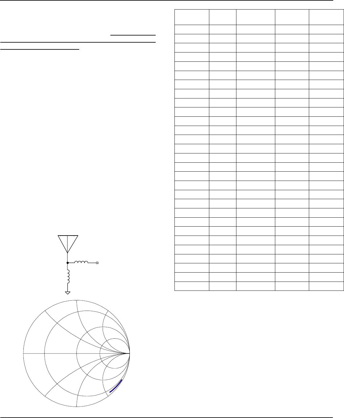
Increasing Selectivity with an Optional BandPass
Filter
For applications located in high ambient noise
environments, a fixed value band-pass network may be
connected between the ANT pin and V
SSRF
to provide
additional receive selectivity and input overload protection.
A minimum input configuration is included in Figure 7 it
provides some filtering and necessary overload protection.
Data Squelching
During quiet periods (no signal) the data output (DO pin)
transitions randomly with noise. Most decoders can
discriminate between this random noise and actual data but
for some system it does present a problem. There are three
possible approaches to reducing this output noise:
1. Analog squelch to raise the demodulator threshold
2. Digital squelch to disable the output when data is
not present
3. Output filter to filter the (high frequency) noise
glitches on the data output pin.
The simplest solution is add analog squelch by introducing
a small offset, or squelch voltage, on the C
TH
pin so that
noise does not trigger the internal comparator. Usually
20mV to 30mV is sufficient, and may be achieved by
connecting a several-megohm resistor from the C
TH
pin to
either V
SS
or V
DD
, depending on the desired offset polarity.
Since the MICRF002 has receiver AGC noise at the
internal comparator input is always the same, set by the
AGC. The squelch offset requirement does not change as
the local noise strength changes from installation to
installation. Introducing squelch will reduce sensitivity and
also reduce range. Only introduce an amount of offset
sufficient to quiet the output. Typical squelch resistor values
range from 6.8MΩ to 10MΩ.
Wake-Up Function
The WAKEB output signal can be used to reduce system
power consumption by enabling the rest of a system when
an RF signal is present. The WAKEB is an output logic
signal which goes active low when the IC detects a
constant RF carrier. The wake-up function is unavailable
when the IC is in shutdown mode.
To activate the Wake-Up function, a received constant RF
carrier must be present for 128 counts or the internal
system clock. The internal system clock is derived from the
reference oscillator and is 1/256 the reference oscillator
frequency. For example:
f
T
= 6.4MHz
f
S
= f
T
/256 = 25kHz
P
S
= 1/f
S
= 0.04ms
128 counts x 0.04ms = 5.12ms
where:
f
T
= reference oscillator frequency
f
S
= system clock frequency
P
S
= system clock period
The Wake-Up counter will reset immediately after a
detected RF carrier drops. The duration of the Wake-Up
signal output is then determined by the required wake up
time plus an additional RF carrier on time interval to create
a wake up pulse output.
WAKEB Output Pulse Time = T
WAKE
+ Additional
RF Carrier On Time
For designers who wish to use the wakeup function while
squelching the output, a positive squelching offset voltage
must be used. This simply requires that the squelch resistor
be connected to a voltage more positive than the quiescent
voltage on the C
TH
pin so that the data output is low in
absence of a transmission.
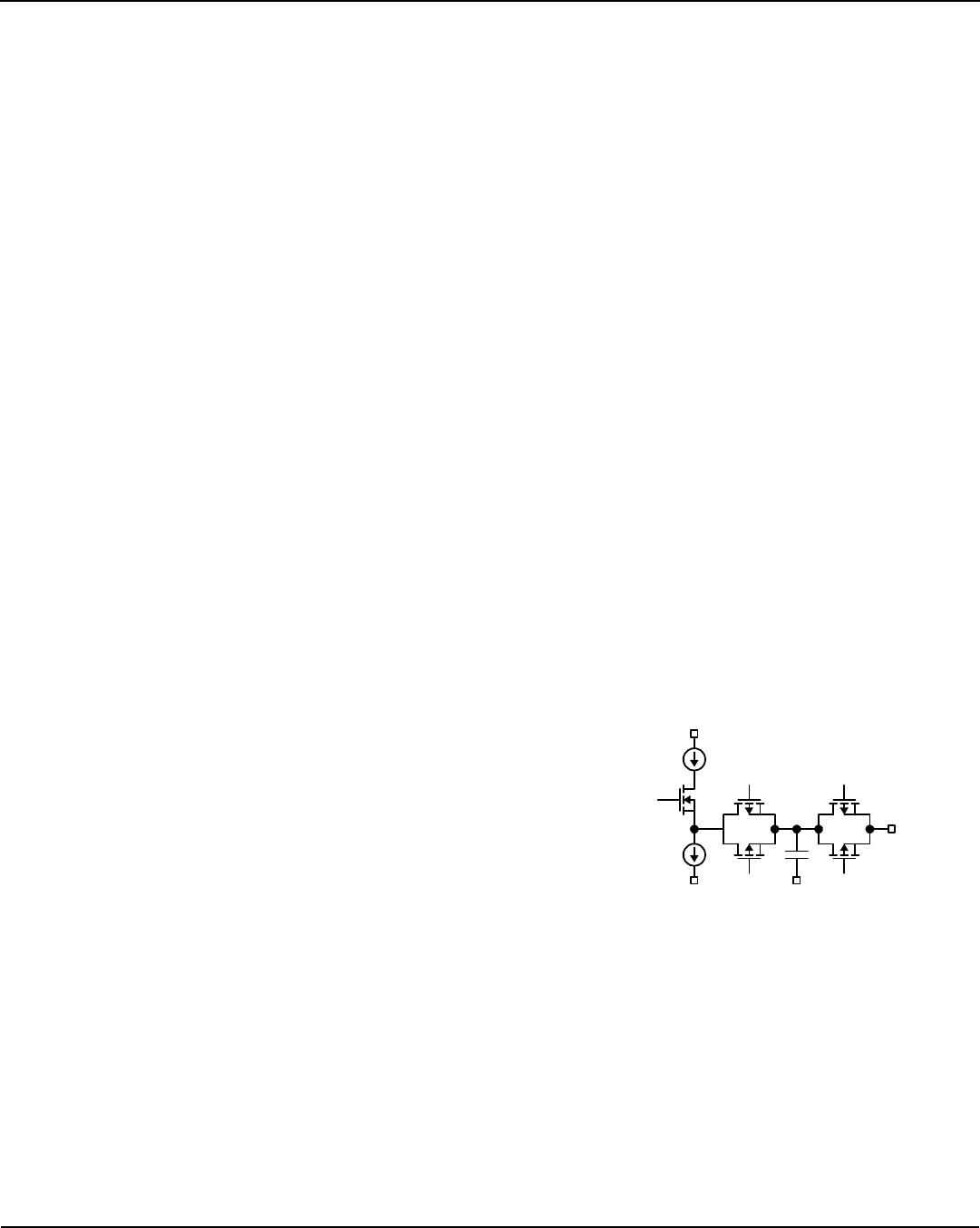
I/O Pin Interface Circuitry
Interface circuitry for the various I/O pins of the MICRF002
are diagrammed in Figures 1 through 6. The ESD
protection diodes at all input and output pins are not shown.
C
TH
Pin
PHI2B PHI1B
PHI1PHI2
CTH
Demodulator
Signal
2.85Vdc
VDDBB
VSSBB VSSBB
Figure 2. CTH Pin
Figure 2 illustrates the C
TH
pin interface circuit. The C
TH
pin
is driven from a P-channel MOSFET source-follower with
approximately 10µA of bias. Transmission gates TG1 and
TG2 isolate the 6.9pF capacitor. Internal control signals
PHI1/PHI2 are related in a manner such that the
impedance across the transmission gates looks like a
“resistance” of approximately 100kΩ. The dc potential at
the C
TH
pin is approximately 1.6V