Micrel, Inc. MICRF002/RF022
July 2008
4
M9999-070808
Absolute Maximum Ratings
(1)
Supply Voltage (V
DDRF
, V
DDBB
)........................................+7V
Input/Output Voltage (V
I/O
). ....................V
SS
–0.3 to V
DD
+0.3
Junction Temperature (T
J
) ....................................... +150°C
Storage Temperature (T
s
) ........................... –65°C to 150°C
Lead Temperature (soldering, 10 sec.)...................... 260°C
ESD Rating
(3)
Operating Ratings
(2)
Supply Voltage (V
DDRF
, V
DDBB
).................... +4.75V to +5.5V
RF Frequency Range.............................. 300MHz to 440Hz
Data Duty-Cycle ................................................20% to 80%
Reference Oscillator Input Range.............. 0.1V
PP
to 1.5V
PP
Ambient Temperature (T
A
) .......................... –40°C to +85°C
Electrical Characteristics
(4)
V
DDRF
= V
DDBB
= V
DD
where +4.75V V
DD
5.5V, V
SS
= 0V; C
AGC
= 4.7µF, C
TH
= 100nF; SEL0 = SEL1 = V
SS
; fixed mode
(SWEN = V
SS
); f
REFOSC
= 4.8970MHz (equivalent to f
RF
= 315MHz); data-rate = 1kbps (Manchester encoded). T
A
= 25°C,
bold values indicate –40°C T
A
+85°C; current flow into device pins is positive; unless noted.
Symbol Parameter Condition Min Typ Max Units
continuous operation, f
RF
= 315MHz 2.2
3.2
mA I
OP
Operating Current
polled with 10:1 duty cycle, f
RF
= 315MHz 220 µA
continuous operation, f
RF
= 433.92MHz 3.5 mA
polled with 10:1 duty cycle, f
RF
= 433.92MHz 350 µA
I
STBY
Standby Current V
SHUT
= V
DD
0.9 µA
RF Section, IF Section
Receiver Sensitivity (
Note 4)
f
RF
= 315MHz –97 dBm
f
RF
= 433.92MHz –95 dBm
f
IF
IF Center Frequency
Note 6
0.86 MHz
f
BW
IF Bandwidth
Note 6
0.43 MHz
Maximum Receiver Input R
SC
= 50 –20 dBm
Spurious Reverse Isolation
ANT pin, R
SC
= 50, Note 5
30 µV
RMS
AGC Attack to Decay Ratio t
ATTACK
÷ t
DECAY
0.1
AGC Leakage Current T
A
= +85°C ±100 nA
Reference Oscillator
Z
REFOSC
Reference Oscillator Input
Impedance
Note 8
290 k
Reference Oscillator Source
Current
5.2 µA
Demodulator
Z
CTH
CTH Source Impedance
Note 7
145 k
I
ZCTH(leak)
CTH Leakage Current T
A
= +85°C ±100 nA
Demodulator Filter Bandwidth
Sweep Mode
(SWEN = VDD or OPEN)
Note 6
V
SEL0
= V
DD
. V
SEL1
= V
DD
V
SEL0
= V
SS
. V
SEL1
= V
DD
V
SEL0
= V
DD
. V
SEL1
= V
SS
V
SEL0
= V
SS
. V
SEL1
= V
SS
4000
2000
1000
500
Hz
Hz
Hz
Hz
Demodulator Filter Bandwidth
Fixed Mode
(SWEN = VSS)
Note 6
V
SEL0
= V
DD
. V
SEL1
= V
DD
V
SEL0
= V
SS
. V
SEL1
= V
DD
V
SEL0
= V
DD
. V
SEL1
= V
SS
V
SEL0
= V
SS
. V
SEL1
= V
SS
8000
4000
2000
1000
Hz
Hz
Hz
Hz
Micrel, Inc. MICRF002/RF022
July 2008
5
M9999-070808
Symbol Parameter Condition Min Typ Max Units
Digital/Control Section
V
IN(high)
Input-High Voltage SEL0, SEL1, SWEN
0.8
V
DD
V
IN(low)
Input-Low Voltage SEL0, SEL1, SWEN
0.2
V
DD
I
OUT
Output Current DO, WAKEB pins, push-pull
10
µA
V
OUT(high)
Output High Voltage DO, WAKEB pins, I
OUT
= –1µA
0.9
V
DD
V
OUT(low)
Output Low Voltage DO, WAKEB pins, I
OUT
= +1µA
0.1
V
DD
t
R
, t
F
Output Rise and Fall Times DO, WAKEB pins, C
LOAD
= 15pF 10 µs
Notes:
1. Exceeding the absolute maximum rating may damage the device.
2. The device is not guaranteed to function outside its operating rating.
3. Devices are ESD sensitive, use appropriate ESD precautions. Meets class 1 ESD test requirements, (human body model HBM), in accordance with
MIL-STD-883C, method 3015. Do not operate or store near strong electrostatic fields.
4. Sensitivity is defined as the average signal level measured at the input necessary to achieve 10-2 BER (bit error rate). The RF input is assumed to be
matched to 50.
5. Spurious reverse isolation represents the spurious components which appear on the RF input pin (ANT) measured into 50 with an input RF
matching network.
6. Parameter scales linearly with reference oscillator frequency f
T
. For any reference oscillator frequency other than 4.8970MHz, compute new
parameter value as the ratio:.
4.8970MHz) at value (parameter
4.8970MHz
MHz
REFOSC
f
×
7. Parameter scales inversely with reference oscillator frequency f
T
. For any reference oscillator frequency other than 4.8970MHz, compute new
parameter value as the ratio:
4.8970MHz) at value (parameter
MHz
REFOSC
f
4.8970MHz
×
8. Series resistance of the resonator (ceramic resonator or crystal) should be minimized to the extent possible. In cases where the resonator series
resistance is too great, the oscillator may oscillate at a diminished peak-to-peak level, or may fail to oscillate entirely. Micrel recommends that series
resistances for ceramic resonators and crystals not exceed 50Ohms and 100 respectively. Refer to Application Hint 35 for crystal
recommendations.
Micrel, Inc. MICRF002/RF022
July 2008
6
M9999-070808
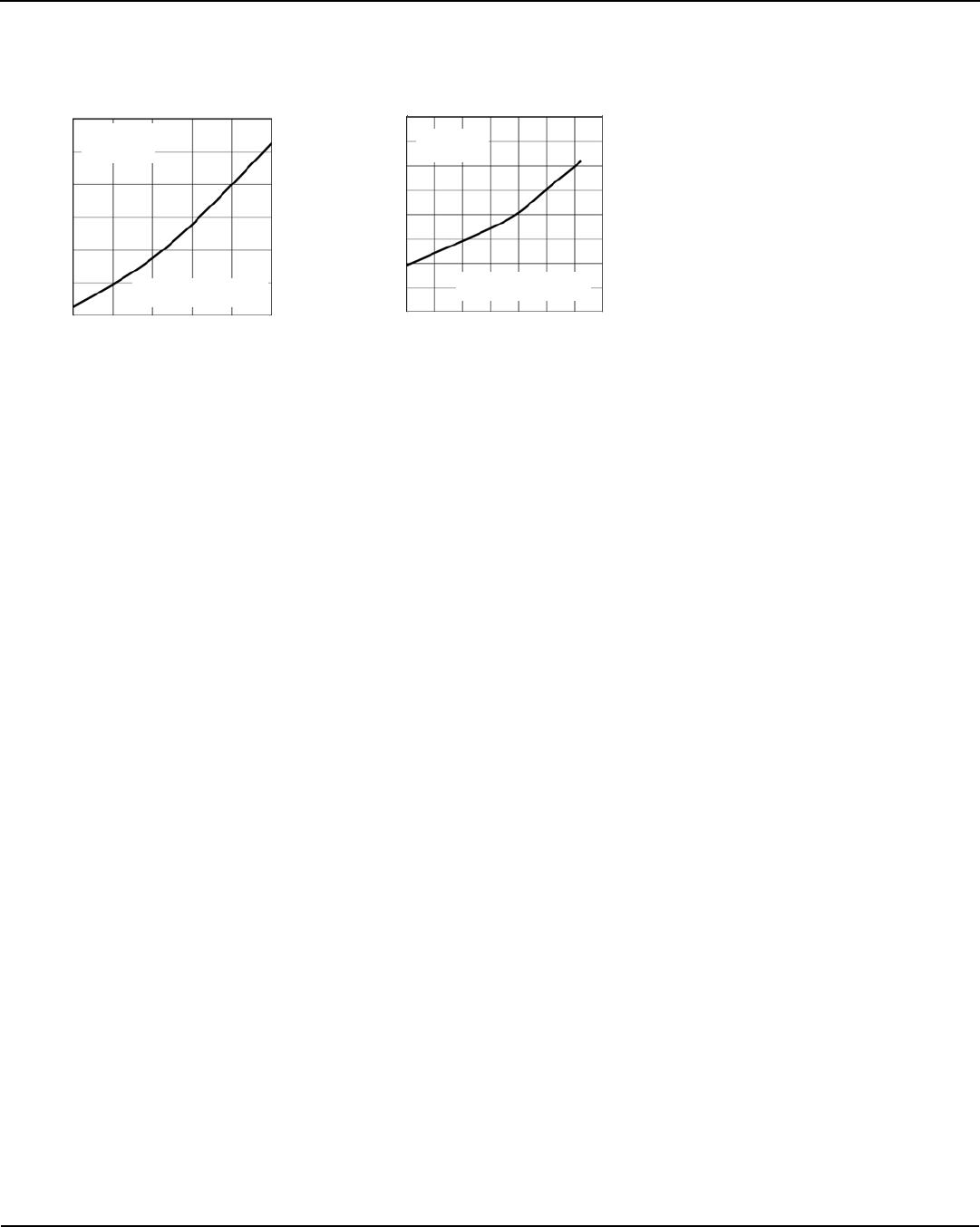
Typical Characteristics
1.5
3.0
4.5
6.0
250 300 350 400 450 500
CURRENT (mA)
FREQUENCY (MHz)
Supply Current
vs. Frequency
T
A
=25°C
V
DD
=5V
Sweep Mode,
Continuous Operation
1.5
2.0
2.5
3.0
3.5
-40 -20 0 20 40 60 80 100
CURRENT (mA)
TEMPERATURE (°C)
Supply Current
vs. Temperature
f = 315MHz
V
DD
=5V
Sweep Mode,
Continuous Operation

MICRF002YM

Mfr. #:
Manufacturer:
Microchip Technology / Micrel
Description:
RF Receiver (Not Recommended for New Designs)300-440MHz RF Receiver With Shutdown
Lifecycle:
New from this manufacturer.
Delivery:
DHL FedEx Ups TNT EMS
Payment:
T/T Paypal Visa MoneyGram Western Union