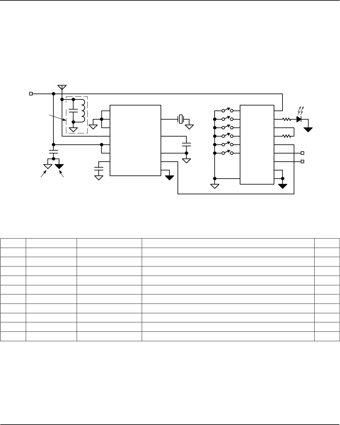
Micrel, Inc. MICRF002/RF022
July 2008 13
M9999-070808
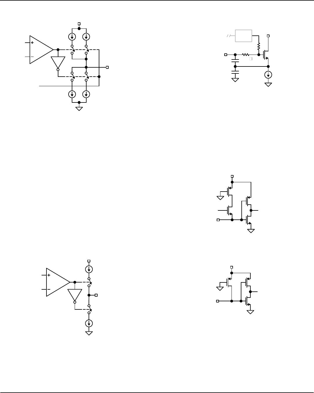
C
AGC
Pin
VDDBB
VSSBB
675µA
67.5µA
Compa-
rator
1.5µA
15µA
Timout
CAG
Figure 3. CAGC Pin
Figure 3 illustrates the C
AGC
pin interface circuit. The AGC
control voltage is developed as an integrated current into a
capacitor C
AGC
. The attack current is nominally 15µA, while
the decay current is a 1/10th scaling of this, nominally
1.5µA, making the attack/decay time constant ratio a fixed
10:1. Signal gain of the RF/IF strip inside the IC diminishes
as the voltage at C
AGC
decreases. Modification of the
attack/decay ratio is possible by adding resistance from the
C
AGC
pin to either V
DDBB
or V
SSBB
, as desired.
Both the push and pull current sources are disabled during
shutdown, which maintains the voltage across C
AGC
, and
improves recovery time in duty-cycled applications. To
further improve duty-cycle recovery, both push and pull
currents are increased by 45 times for approximately 10ms
after release of the SHUT pin. This allows rapid recovery of
any voltage droop on C
AGC
while in shutdown.
DO and WAKEB Pins
VDDBB
VSSBB
Compa-
rator
10µA
10µA
DO
Figure 4. DO and WAKEB Pins
The output stage for DO (digital output) and WAKEB
(wakeup output) is shown in Figure 4. The output is a 10µA
push and 10µA pull switched-current stage. This output
stage is capable of driving CMOS loads. An external buffer-
driver is recommended for driving high-capacitance loads.
REFOSC Pin
250
200k
Active
Bias
REFOSC
30pF
30pF
30µA
VDDBB
VSSBB
VSSB
Figure 5. REFOSC Pin
The REFOSC input circuit is shown in Figure 5. Input
impedance is high (200kΩ). This is a Colpitts oscillator with
internal 30pF capacitors. This input is intended to work with
standard ceramic resonators connected from this pin to the
V
SSBB
pin, although a crystal may be used when greater
frequency accuracy is required. The nominal dc bias
voltage on this pin is 1.4V.
SEL0, SEL1, SWEN, and SHUT Pins
to Interna
Circuits
VDDBB
VSSBB
SEL0,
SEL1,
SWEN
Q2
Q3
Q1
VSSBB
SHUT
Q4
Figure 6a. SEL0, SEL1, SWEN Pins
to Interna
Circuits
VDDBB
VSSBB
SHUT
Q2
Q3
Q1
VSSBB
Figure 6b. SHUT Pin
Control input circuitry is shown in Figures 6a and 6b. The
standard input is a logic inverter constructed with minimum
geometry MOSFETs (Q2, Q3). P-channel MOSFET Q1 is
a large channel length device which functions essentially
as a “weak” pullup to V
DDBB
. Typical pull-up current is 5µA,
leading to an impedance to the V
DDBB
supply of typically
1MΩ.