LTC4370
1
4370f
Typical applicaTion
FeaTures DescripTion
Two-Supply Diode-OR
Current Balancing Controller
The LTC
®
4370 is a two-supply current sharing controller
which incorporates MOSFET ideal diodes. The diodes
block reverse and shoot-through currents during start-up
and fault conditions. Their forward voltage is adjusted to
share the load currents between supplies. Unlike other
sharing methods, neither a share bus nor trim pins on
the supply are required.
The maximum MOSFET voltage drop can be set with a
resistor. A fast gate turn-on reduces the load voltage
droop during supply switchover. If the input supply fails
or is shorted, a fast turn-off minimizes reverse current
transients.
The controller operates with supplies from 2.9V to 18V.
For lower rail voltages, an external supply is needed at
the V
CC
pin. Enable inputs can be used to turn off the
MOSFET and put the controller in a low current state.
Status outputs indicate whether the MOSFETs are on or
off. The load sharing function can be disabled to turn the
LTC4370 into a dual ideal diode controller.
12V, 10A Load Share Current Sharing Error vs Supply Difference
applicaTions
n
Shares Load Between Two Supplies
n
Eliminates Need for Active Control of
Input Supplies
n
No Share Bus Required
n
Blocks Reverse Current
n
No Shoot-Through Current During Start-Up or Faults
n
0V to 18V High Side Operation
n
Enable Inputs
n
MOSFET On Status Outputs
n
Dual Ideal Diode Mode
n
16-Lead DFN (4mm × 3mm) and MSOP Packages
n
Redundant Power Supplies
n
High Availability Systems and Servers
n
Telecom and Network Infrastructure
L, LT, LTC , LT M, Linear Technology and the Linear logo are registered trademarks and
PowerPath and ThinSOT are trademarks of Linear Technology Corporation. All other trademarks
are the property of their respective owners. Protected by U.S. Patents, including 7920013 and
8022679. Additional patent pending.
SUM85N03-06P
*OPTIONAL, FOR FAST TURN-ON
SUM85N03-06P
GATE1CPO1
CPO2
GND
EN1
EN2
RANGE
4370 TA01
V
INA
12V
V
INB
12V
0.1µF
NC
OUT
12V, 10A
39nF*
39nF*
V
IN1
V
CC
FETON1
COMP
FETON2
OUT1
OUT2
GATE2
V
IN2
LTC4370
2mΩ
2mΩ
0.18µF
V
INA
– V
INB
(mV)
–750
–20
SHARING ERROR (I
VINA
I
VINB
)/I
L
(%)
–10
0
10
–500 –250 2500 500
20
–15
–5
5
15
750
4370 TA01b
LTC4370
2
4370f
absoluTe MaxiMuM raTings
V
IN1
, V
IN2
, OUT1, OUT2 Voltages ...................−2V to 24V
V
CC
Voltage ............................................... 0.3V to 6.5V
GATE1, GATE2 Voltages (Note 3) ............... 0.3V to 34V
CPO1, CPO2 Voltages (Note 3) ................... 0.3V to 34V
RANGE Voltage ................................0.3V to V
CC
+ 0.3V
COMP Voltage .............................................. 0.3V to 3V
EN1, EN2, FETON1, FETON2 Voltages .........0.3V to 24V
CPO1, CPO2 Average Current .................................10mA
(Notes 1, 2)
16
15
14
13
12
11
10
9
17
1
2
3
4
5
6
7
8
EN1
GND
V
CC
V
IN1
GATE1
CPO1
OUT1
FETON1
EN2
RANGE
COMP
V
IN2
GATE2
CPO2
OUT2
FETON2
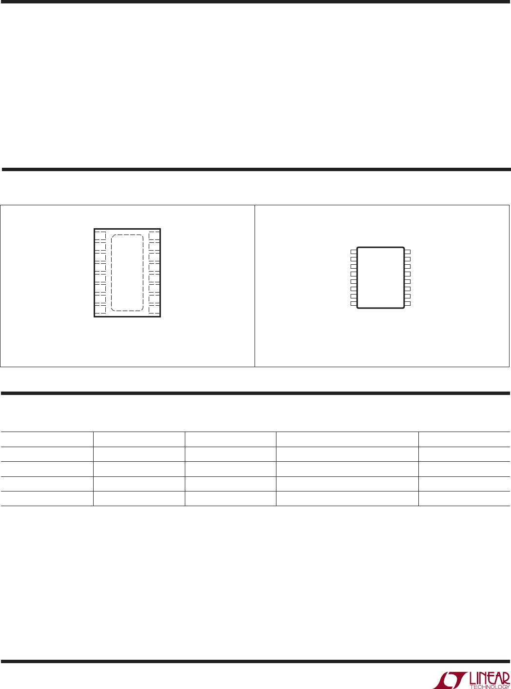
TOP VIEW
DE PACKAGE
16-LEAD (4mm × 3mm) PLASTIC DFN
T
JMAX
= 125°C, θ
JA
= 43°C/W
EXPOSED PAD (PIN 17) PCB GND CONNECTION IS OPTIONAL
1
2
3
4
5
6
7
8
EN2
RANGE
COMP
V
IN2
GATE2
CPO2
OUT2
FETON2
16
15
14
13
12
11
10
9
EN1
GND
V
CC
V
IN1
GATE1
CPO1
OUT1
FETON1
TOP VIEW
MS PACKAGE
16-LEAD PLASTIC MSOP
T
JMAX
= 125°C, θ
JA
= 125°C/W
pin conFiguraTion
orDer inForMaTion
LEAD FREE FINISH TAPE AND REEL PART MARKING* PACKAGE DESCRIPTION TEMPERATURE RANGE
LTC4370CDE#PBF LTC4370CDE#TRPBF 4370 16-Lead (4mm × 3mm) Plastic DFN 0°C to 70°C
LTC4370IDE#PBF LTC4370IDE#TRPBF 4370 16-Lead (4mm × 3mm) Plastic DFN –40°C to 85°C
LTC4370CMS#PBF LTC4370CMS#TRPBF 4370 16-Lead Plastic MSOP 0°C to 70°C
LTC4370IMS#PBF LTC4370IMS#TRPBF 4370 16-Lead Plastic MSOP –40°C to 85°C
Consult LTC Marketing for parts specified with wider operating temperature ranges. *The temperature grade is identified by a label on the shipping container.
For more information on lead free part marking, go to: http://www.linear.com/leadfree/
For more information on tape and reel specifications, go to: http://www.linear.com/tapeandreel/
FETON1, FETON2 Currents .......................................5mA
Operating Ambient Temperature Range
LTC4370C ................................................ 0°C to 70°C
LTC4370I .............................................−40°C to 85°C
Storage Temperature Range .................. 65°C to 150°C
Lead Temperature (Soldering, 10 sec)
MS Package ......................................................300°C
LTC4370
3
4370f
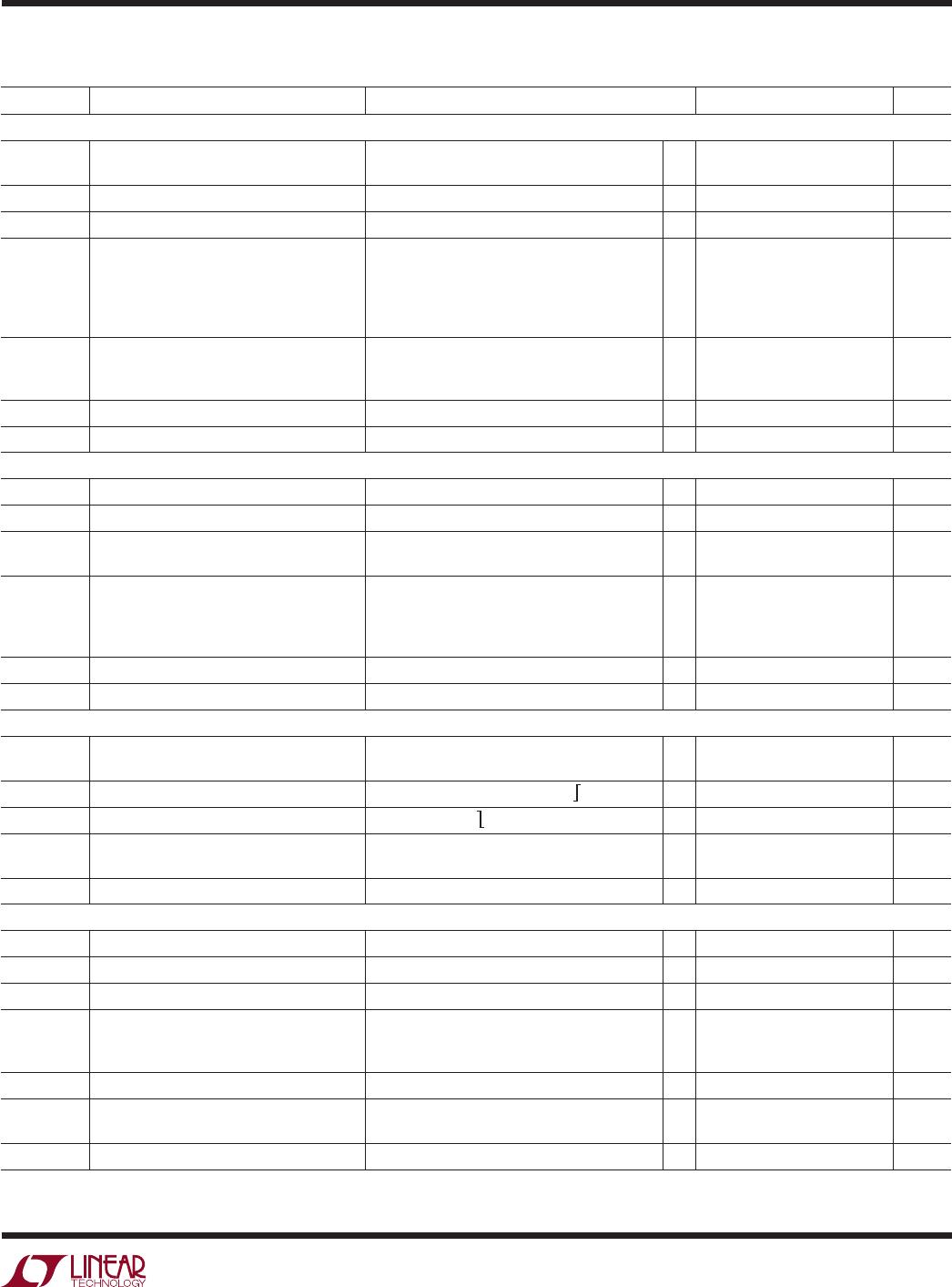
elecTrical characTerisTics
The l denotes those specifications which apply over the full operating
temperature range, otherwise specifications are at T
A
= 25°C. V
IN1
= V
IN2
= 12V, OUT = V
IN
, V
CC
open, unless otherwise noted.
SYMBOL PARAMETER CONDITIONS MIN TYP MAX UNITS
Supplies
V
IN
V
IN1
, V
IN2
Operating Range
With External V
CC
Supply
l
l
2.9
0
18
V
CC
V
V
V
CC(EXT)
V
CC
External Supply Operating Range V
IN1
, V
IN2
≤ V
CC
l
2.9 6 V
V
CC(REG)
V
CC
Regulated Voltage
l
4.5 5 5.5 V
I
IN
V
IN1
, V
IN2
Current
Enabled, Higher Supply
Enabled, Lower Supply
Pull-Up
Disabled
Other V
IN
= 11.7V, Both EN = 0V
Other V
IN
= 12.3V, Both EN = 0V
Both V
IN
= 0V, V
CC
= 5V, Both EN = 0V
Both EN = 1V
l
l
l
l
2.1
320
–110
80
3
450
–180
180
mA
µA
µA
µA
I
CC
V
CC
Current
Enabled
Disabled
V
CC
= 5V, Both V
IN
= 1.2V, Both EN = 0V
V
CC
= 5V, Both V
IN
= 1.2V, Both EN = 1V
l
l
2
105
2.8
220
mA
µA
V
CC(UVLO)
V
CC
Undervoltage Lockout Threshold V
CC
Rising
l
2.3 2.55 2.7 V
ΔV
CC(HYST)
V
CC
Undervoltage Lockout Hysteresis
l
40 120 300 mV
Load Share
V
EA(OS)
Error Amplifier Input Offset
l
0 ±2 mV
g
m(EA)
Error Amplifier Gain (–ΔI
COMP
/ΔV
OUT
) 150 µS
V
FR(MIN)
Minimum Forward Regulation Voltage
(V
IN
– OUT)
V
IN
= 1.2V, V
CC
= 5V
V
IN
= 12V
l
l
2
2
12
25
25
50
mV
mV
V
FR(MAX)
Maximum Forward Regulation Voltage
(V
IN
– OUT)
R
RANGE
= 4.99k, V
IN
= 1.2V, V
CC
= 5V
R
RANGE
= 4.99k, V
IN
= 12V
R
RANGE
= 49.9k, V
IN
= 1.2V, V
CC
= 5V
R
RANGE
= 49.9k, V
IN
= 12V
l
l
l
l
40
45
425
440
62
75
511
524
82
100
575
590
mV
mV
mV
mV
I
RANGE
RANGE Pull-Up Current RANGE = 0.2V
l
–8.8 –10 –11.2 µA
V
RANGE(TH)
RANGE Load Share Disable Threshold
l
V
CC
– 0.5 V
CC
– 0.3 V
CC
– 0.1 V
Gate Drive
ΔV
GATE
MOSFET Gate Drive (GATE – V
IN
) V
FWD
= 0.2V; I = 0, −1μA; Highest V
IN
= 12V
V
FWD
= 0.2V; I = 0, −1μA; Highest V
IN
= 2.9V
l
l
10
4.5
12
7
14
9
V
V
t
ON(GATE)
GATE1, GATE2 Turn-On Propagation Delay
V
FWD
(= V
IN
– OUT) Step: –0.3V
0.3V
l
0.4 1 µs
t
OFF(GATE)
GATE1, GATE2 Turn-Off Propagation Delay
V
FWD
Step: 0.3V
0.3V
l
0.4 1 µs
I
GATE(PK)
GATE1, GATE2 Peak Pull-Up Current
GATE1, GATE2 Peak Pull-Down Current
V
FWD
= 0.4V, ΔV
GATE
= 0V, CPO = 17V
V
FWD
= −2V, ΔV
GATE
= 5V
l
l
–0.9
0.9
–1.4
1.4
–1.9
1.9
A
A
I
GATE(OFF)
GATE1, GATE2 Off Pull-Down Current Corresponding EN = 1V, ΔV
GATE
= 2.5V
l
65 110 160 µA
Input/Output Pins
V
EN(TH)
EN1, EN2 Threshold Voltage EN Falling
l
580 600 620 mV
ΔV
EN(TH)
EN1, EN2 Threshold Hysteresis
l
2 8 20 mV
I
EN
EN1, EN2 Current At 0.6V
l
0 ±1 µA
I
OUT
OUT1, OUT2 Current
Enabled
Disabled
OUT
n
= 0V, 12V; Both EN = 0V
Both EN = 1V
l
l
–70
16
260
40
µA
µA
I
CPO(UP)
CPO1, CPO2 Pull-Up Current CPO = V
IN
l
–40 –70 –115 µA
V
OL
FETON1, FETON2 Output Low Voltage I = 1mA
I = 3mA
l
l
0.12
0.36
0.4
1.2
V
V
V
OH
FETON1, FETON2 Output High Voltage I = −1μA, V
FWD
= 1V
l
V
CC
– 1.4 V
CC
– 0.9 V
CC
– 0.5 V

LTC4370CMS#PBF

Mfr. #:
Manufacturer:
Analog Devices Inc.
Description:
Power Management Specialized - PMIC Two-S Diode-OR C Balancing Cntr
Lifecycle:
New from this manufacturer.
Delivery:
DHL FedEx Ups TNT EMS
Payment:
T/T Paypal Visa MoneyGram Western Union