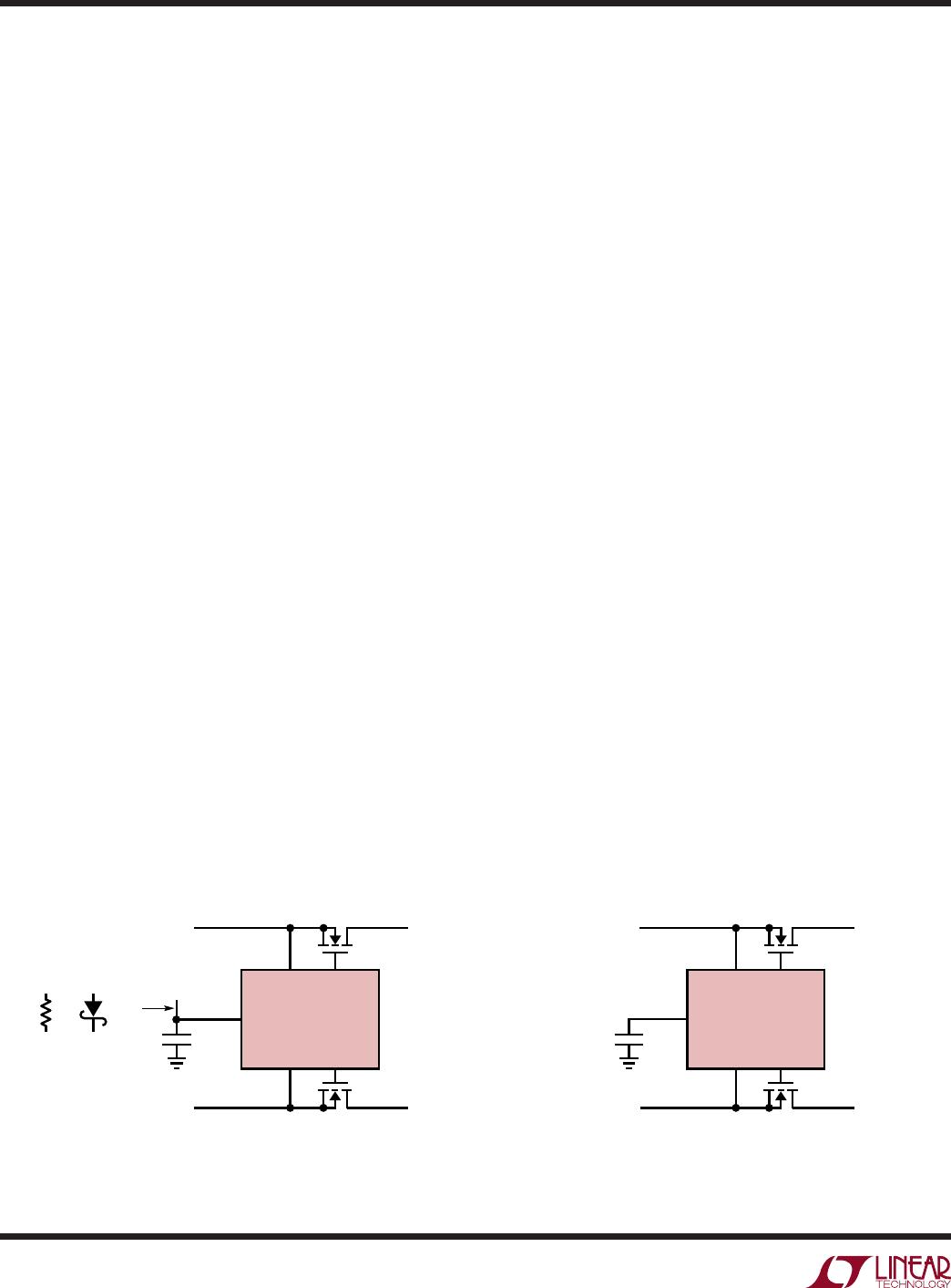
LTC4370
10
4370f
diverging, and so too, the supply currents. As the supply
voltages separate, the entire load current is steered to the
higher supply. Now, the servo command across the higher
supply’s MOSFET is folded back from the maximum to
the minimum servo to minimize power dissipated in the
MOSFET. The sharing capture range, ΔV
IN(SH)
, in Figure2a
is ±500mV, set by V
RANGE
. Figure 2b will be discussed
later in the MOSFET Selection section.
RANGE Pin Configuration
The RANGE pin resistor is decided by the design trade-off
between the sharing capture range and the power dissipated
in the MOSFET. A larger R
RANGE
increases the capture
range at the expense of enhanced power dissipation and
reduced load voltage. On the other hand, supplies with
tight tolerances can afford a smaller capture range and
therefore cooler operation of the MOSFETs.
As mentioned, the upper limit of the servo command ad-
justment is V
RANGE
plus the minimum forward regulation
voltage. Since an internal 10μA pull-up current flowing
through the external resistor sets V
RANGE
:
V
FR(MAX)
= 10µAR
RANGE
+ V
FR(MIN)
(1)
If R
RANGE
is larger than 60k (including the pin open
state), the internal limit for the first term on the right-
hand
side of Equation 1 is 600mV, setting V
FR(MAX)
to
612mV or 625mV. Note that servo voltages nearing the
MOSFET’s body diode voltage may divert some or all cur-
rent to the diode especially at hot temperatures. This may
either cause FETON to go low if V
GS
falls below 0.7V, or
loss of sharing control. Also note that an open RANGE pin
biases itself to a voltage greater than 600mV.
Connecting the RANGE pin to V
CC
disables the load sharing
loop. The servo voltages for both MOSFETs are fixed at the
minimum with no adjustment. The device now behaves
as a dual ideal diode controller. This is handy for testing
purposes. Use the LTC4353 if only a dual ideal diode
controller is needed.
Power Supply Configuration
The LTC4370 can load share high side supplies down to
0V rail voltage. This requires powering the V
CC
pin with an
early external supply in the 2.9V to 6V range. In this range
of operation V
IN
should be lower than V
CC
. If V
CC
powers
up after V
IN
, and backfeeding of V
CC
by the internal 5V LDO
is a concern, then a series resistor (few 100Ω) or Schottky
diode
limits device power dissipation and backfeeding of
a low V
CC
supply when any V
IN
is high. A 0.1µF bypass
capacitor should also be connected between the V
CC
and
GND pins, close to the device. Figure 3 illustrates this.
If either V
IN
operates above 2.9V, then the external supply
at V
CC
is not needed. The 0.1µF capacitor is still required
for bypassing.
Start of Sharing
When currents are not being shared either because the
load current or one of the supplies is off, the COMP volt-
age is railed towards 0V or 2V depending on the input
signal to the error amplifier and its offset. For example,
applicaTions inForMaTion
Figure 3. Power Supply Configurations
GATE1
4370 F03
0V TO V
CC
0V TO
V
CC
V
IN1
V
CC
GATE2
V
IN2
LTC4370
2.9V TO 6V
GATE1
M1
M2
M1
M2
2.9V TO 18V
(0V TO 18V)
0V TO 18V
(2.9V TO 18V)
V
IN1
V
CC
GATE2
V
IN2
LTC4370
C
VCC
0.1µF
C
VCC
0.1µF
OPTIONAL
OR HERE
LTC4370
11
4370f
in the absence of load current the differential input volt-
age to the error amplifier is zero and the COMP current is
g
m(EA)
V
EA(OS)
. Before sharing can start, the COMP
voltage has to slew towards its operating point of 0.7V
(when V
IN1
< V
IN2
) or 1.24V (V
IN1
> V
IN2
). This delay is
determined by the differential input signal to the error
amplifier (which is ΔV
OUT
= OUT1 – OUT2 = (I
1
I
2
) R
S
),
its g
m
and the COMP capacitor value. Depending on how
the currents split before converging, the delay can vary
from 1 to 5 times:
C
C
ΔV
COMP
g
m(EA)
I
L
R
S
Figure 4a shows the case where a 5.1V V
IN1
is turned
on while V
IN2
is at 4.9V supplying 10A. Initially, COMP
is railed low to 0.1V since ΔV
OUT
(−I
2
R
S
) is negative,
and needs to rise to 1.24V as the final V
IN1
is higher than
V
IN2
. With V
IN1
off, ΔV
IN
is large and negative, causing the
forward regulation voltage of the second supply V
FR2
to be
folded back to the minimum V
FR(MIN)
(travelling from left
to right in Figure 2a). As the ΔV
IN
magnitude decreases,
V
FR2
rises to the maximum V
FR(MAX)
, lowering I
2
and the
load voltage. COMP is around 0.7V when V
FR2
is being
adjusted. When COMP reaches 1.24V, V
FR2
is kept at the
minimum and V
FR1
is adjusted appropriately to compensate
for the 0.2V of ΔV
IN
. The sharing closure is smoother for
the case where V
IN1
< V
IN2
since COMP only has to slew
to 0.7V to lower V
FR2
(Figure 4b).
MOSFET Selection
The LTC4370 drives N-channel MOSFETs to conduct the
load current. The important parameters of the MOSFET
are its maximum drain-source voltage BV
DSS
, maximum
gate-source voltage
V
GS(MAX)
, on-resistance R
DS(ON)
, and
maximum power dissipation P
D(MAX)
.
If an input is connected to ground, the full supply voltage
can appear across the MOSFET. To survive this, the BV
DSS
must be higher than the supply voltages. The V
GS(MAX)
rating of the MOSFET should exceed 14V since that is the
upper limit of the internal GATE to V
IN
clamp.
To obtain the maximum sharing capture range, the R
DS(ON)
should be low enough for the servo amplifier to regulate the
minimum forward regulation voltage across the MOSFET
while it’s conducting half of the load current. If it cannot,
the gate voltage will be railed high. Hence, the R
DS(ON)
value
in the MOSFET data sheet should be looked up for 10V or
4.5V gate drive depending on the V
IN
voltage. Since the
OUT voltages are equal, the breakpoint for exact sharing
in the higher R
DS(ON)
case is:
ΔV
IN(SH)
= V
FR(MAX)
– 0.5I
L
R
DS(ON)
(2)
applicaTions inForMaTion
Figure 4. Start of Sharing at V
IN1
Turn-On
(4a) V
IN1
> V
IN2
(4b) V
IN1
< V
IN2
CURRENT
5A/DIV
VOLTAGE
2V/DIV
4370 F04a
25ms/DIV
V
IN1
= 5.1V
V
IN2
= 4.9V
I
L
= 10A
I
2
I
1
OUT
COMP
(1V/DIV)
V
IN1
CURRENT
5A/DIV
VOLTAGE
2V/DIV
4370 F04b
25ms/DIV
I
2
I
1
OUT
V
IN1
V
IN1
= 4.9V
V
IN2
= 5.1V
I
L
= 10A
COMP
(0.5V/DIV)
LTC4370
12
4370f
In Figure 2b, 0.5I
L
R
DS(ON)
is 125mV. The higher R
DS(ON)
rails the servo amplifier high as it cannot regulate the 25mV
V
FR(MIN)
across the lower supply’s MOSFET. Compared
to Figure 2a, the sharing capture range shrinks by 100mV
(125mV – 25mV) to ±400mV. However, the ΔV
IN
over
which currents are shared partially stays the same at
500mV + I
L
R
S
. Even when not maximizing sharing range,
I
L
R
DS(ON)
should be kept below 75mV for optimum
performance.
The peak power dissipation in the MOSFET occurs when
the entire load current is being sourced by one supply
with the maximum forward regulation voltage dropped
across the MOSFET (as shown in Figure 2a). Therefore,
the P
D(MAX)
rating of the MOSFET should satisfy:
P
D(MAX)
≥ I
L
V
FR(MAX)
(3)
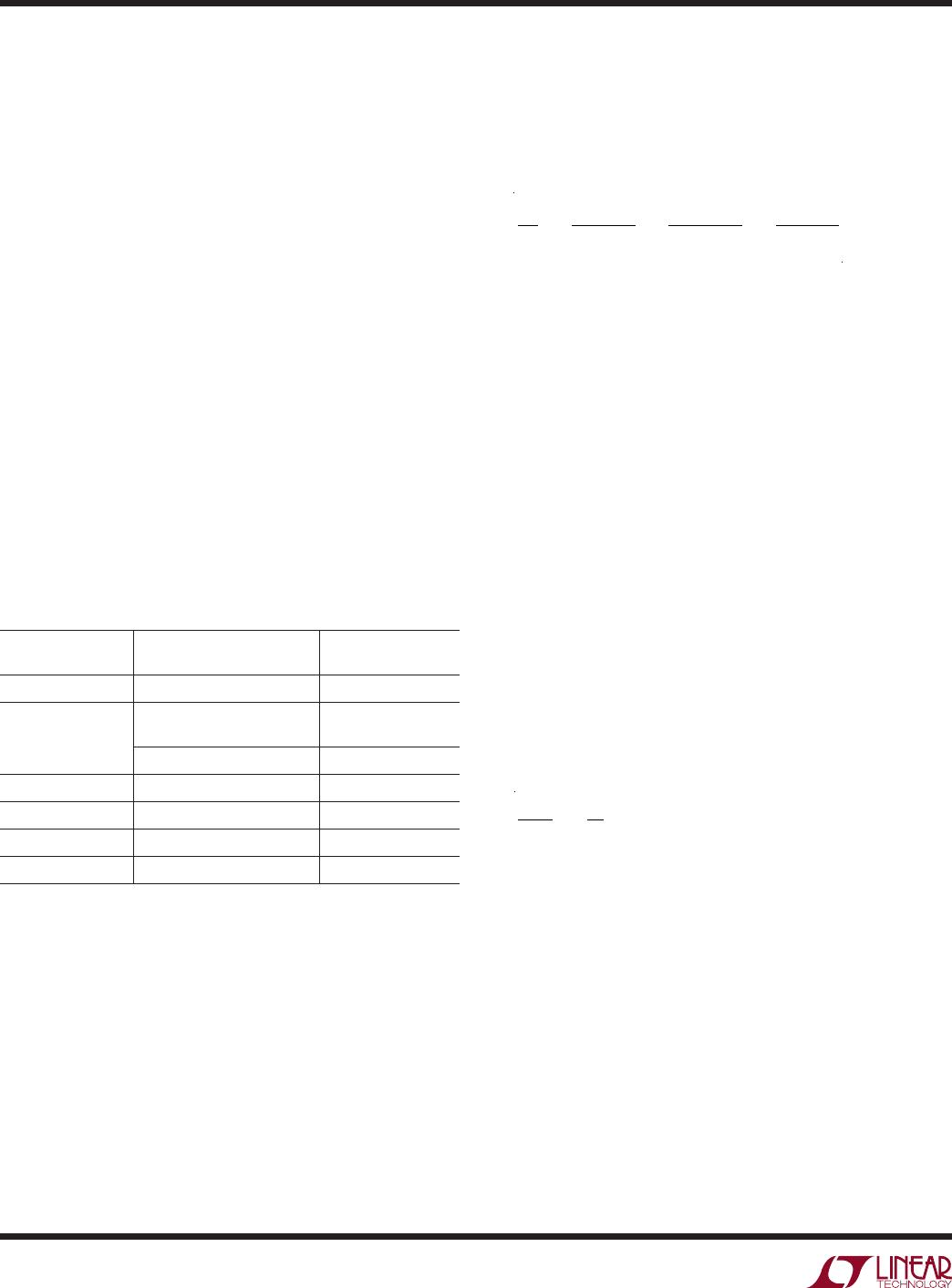
Table 1 provides starting guidelines for the type of
MOSFET package and heat sink required at various levels
of power dissipation. These are typical ranges for a room
temperature ambient with no air flow.
Table 1. Guidelines for MOSFET Power Dissipation
MAXIMUM POWER
DISSIPATED MOSFET PACKAGE HEAT SINK
0.5W to 1W SO-8 PCB
1W to 2W SO-8 With Exposed Pad,
D-Pak (TO-252)
PCB
TO-220 Standing in Free Air
2W to 4W DD-Pak (TO-263), TO-220 PCB
4W to 10W TO-220 Stamping
10W to 20W TO-220 Casting, Extrusion
20W to 50W TO-247, TO-3P Extrusion
Sense Resistor Selection
The sense resistor voltage drop dictates the current sharing
accuracy. Sharing error, due to the error amplifier input
offset, decreases with increasing sense voltage as:
ΔI
I
L
=
|I
1
I
2
|
I
L
=
| V
EA(OS)
|
I
L
R
S
=
2mV
I
L
R
S
(4)
I
1
and I
2
are the two supply currents, I
L
is the load current
(I
1
+ I
2
= I
L
), R
S
is the sense resistor value, and V
EA(OS)
is the input offset of the internal error amplifier. A 25mV
sense resistor voltage drop with half of the load cur-
rent flowing through it (i.e., I
L
R
S
= 50mV) gives a 4%
sharing error. A larger sense resistance may also be
needed if there is a connector in between the OUT pins
and the load to minimize the effect of its resistance. At
larger sense voltages the accuracy will be limited by the
sense resistor tolerance.
If sharing accuracy requirements can be relaxed, power
dissipated in the sense resistor can be reduced by selecting
a lower resistance. Worst-case power dissipation happens
at full load, i.e., when load current is not being shared.
While reducing the sense resistance, note that the sharing
loop does not close for load currents below V
EA(OS)
/R
S
.
The two sense resistors can have different values if the
application does not require the load current to be shared
equally between the supplies. In such a case:
R
S1
R
S2
=
I
2
I
1
(5)
CPO Capacitor Selection
The recommended value of the capacitor between the CPO
and V
IN
pins is approximately 10× the input capacitance C
ISS
of the MOSFET. A larger capacitor takes a correspondingly
longer time to be charged by the internal charge pump. A
smaller capacitor suffers more voltage drop during a fast
gate turn-on event as it shares charge with the MOSFET
gate capacitance.
applicaTions inForMaTion

LTC4370CMS#PBF

Mfr. #:
Manufacturer:
Analog Devices Inc.
Description:
Power Management Specialized - PMIC Two-S Diode-OR C Balancing Cntr
Lifecycle:
New from this manufacturer.
Delivery:
DHL FedEx Ups TNT EMS
Payment:
T/T Paypal Visa MoneyGram Western Union