REV. B
AD7470/AD7472
–10–
CIRCUIT DESCRIPTION
CONVERTER OPERATION
The AD7470/AD7472 are 10-bit/12-bit successive approxima-
tion analog-to-digital converters based around a capacitive
DAC. The AD7470/AD7472 can convert analog input signals in
the range 0 V to V
REF
. Figure 2 shows a very simplified sche-
matic of the ADC. The control logic, SAR, and the capacitive
DAC are used to add and subtract fixed amounts of charge
from the sampling capacitor to bring the comparator back into a
balanced condition.
CAPACITIVE
DAC
SWITCHES
SAR
CONTROL LOGIC
COMPARATOR
OUTPUT DATA
10-/12-BIT PARALLEL
V
IN
V
REF
CONTROL
INPUTS
Figure 2. Simplified Block Diagram of AD7470/AD7472
Figure 3 shows the ADC during its acquisition phase. SW2 is
closed and SW1 is in Position A. The comparator is held in a
balanced condition and the sampling capacitor acquires the
signal on V
IN
.
COMPARATOR
V
IN
CONTROL LOGIC
CAPACITIVE
DAC
AGND
2k
SW2
SW1
A
B
Figure 3. ADC Acquisition Phase
Figure 4 shows the ADC during conversion. When conversion
starts, SW2 will open and SW1 will move to position B, causing
the comparator to become unbalanced. The ADC then runs
through its successive approximation routine and brings the
comparator back into a balanced condition. When the compara-
tor is rebalanced, the conversion result is available in the SAR
register.
COMPARATOR
V
IN
CONTROL LOGIC
CAPACITIVE
DAC
AGND
2k
SW2
SW1
A
B
Figure 4. ADC Conversion Phase
TYPICAL CONNECTION DIAGRAM
Figure 5 shows a typical connection diagram for the AD7470/
AD7472. Conversion is initiated by a falling edge on CONVST.
Once CONVST goes low, the BUSY signal goes high, and at
the end of conversion, the falling edge of BUSY is used to acti-
vate an interrupt service routine. The CS and RD lines are then
activated in parallel to read the 10- or 12-data bits. The recom-
mended REF IN voltage is 2.5 V providing an analog input
range of 0 V to 2.5 V, making the AD7470/AD7472 a unipolar
ADC. It is recommended to perform a dummy conversion after
power-up as the first conversion result could be incorrect. This
also ensures that the part is in the correct mode of operation.
The CONVST pin should not be floating when power is applied
as a rising edge on CONVST might not wake up the part.
In Figure 5 the V
DRIVE
pin is tied to DV
DD
,
which results in logic
output voltage values being either 0 V or DV
DD
. The voltage
applied to V
DRIVE
controls the voltage value of the output logic
signals. For example, if DV
DD
is supplied by a 5 V supply and
V
DRIVE
by a 3 V supply, the logic output voltage levels would be
either 0 V or 3 V. This feature allows the AD7470/AD7472 to
interface to 3 V parts while still enabling the ADC to process
signals at 5 V supply.
10F0.1F
PARALLED
INTERFACE
2.5V*
*RECOMMENDED REF IN VOLTAGE
0V TO
REF IN
1nF
10F 0.1F 47F
AD7470/
AD7472
AV
DD
V
DRIVE
DV
DD
REF IN
DB0–
DB9 (DB11)
CS
BUSY
CONVST
RD
V
IN
C/P
ANALOG
SUPPLY
2.7V–5.25V
++
Figure 5. Typical Connection Diagram
REV. B
AD7470/AD7472
–11–
ADC TRANSFER FUNCTION
The output coding of the AD7470/AD7472 is straight binary.
The designed code transitions occur midway between succes-
sive integer LSB values (0.5 LSB, 1.5 LSB, etc). The LSB
size is equal to (REF IN)/4096 for the AD7472 and to (REF
IN)/1024 for the AD7470. The ideal transfer characteristic for
the AD7472 is shown in Figure 6.
111...111
111...110
111...000
011...111
000...010
000...001
000...000
ADC CODE
0V 0.5LSB V
REF
–1.5LSB
ANALOG INPUT
1LSB = V
REF
/4096
Figure 6. Transfer Characteristic for 12 Bits
AC ACQUISITION TIME
In ac applications it is recommended to always buffer analog
input signals. The source impedance of the drive circuitry must
be kept as low as possible to minimize the acquisition time of
the ADC. Large values of impedance at the V
IN
pin of the ADC
will cause the THD to degrade at high input frequencies.
The AD8021, AD8047, AD8051, AD9631, and AD797 are
some of the op amps that could be used to buffer the analog
input. Figure 7 shows the AD7470/AD7472 performance for
some of those recommended input buffers.
TYPICAL AMPLIFIER
INPUT SNR THD CURRENT
BUFFERS 500kHz 500kHz CONSUMPTION
AD8047 70 78 5.8mA
AD9631 69.5 80 17mA
AD8051 68.6 78 4.4mA
AD797 70 84 8.2mA
AD7470/AD7472
DYNAMIC
PERFORMANCE
SPECIFICATIONS
Figure 7. Recommended Input Buffers
Reference Input
The following references are best suited for use with the
AD7470/AD7472.
ADR291
AD780
REF192
ADR421
For optimum performance, a 2.5 V reference is recommended.
The parts can function with a reference up to 3 V and down to
2 V, but the performance deteriorates.
DC ACQUISITION TIME
The ADC starts a new acquisition phase at the end of a conver-
sion and ends it on the falling edge of the CONVST signal. At
the end of conversion there is a settling time associated with the
sampling circuit. This settling time lasts approximately 135 ns.
The analog signal on V
IN
is also being acquired during this
settling time; therefore, the minimum acquisition time needed is
approximately 135 ns.
Figure 8 shows the equivalent charging circuit for the sampling
capacitor when the ADC is in its acquisition phase. R3 repre-
sents the source impedance of a buffer amplifier or resistive
network, R1 is an internal switch resistance, R2 is for bandwidth
control, and C1 is the sampling capacitor. C2 is back-plate
capacitance and switch parasitic capacitance.
During the acquisition phase the sampling capacitor must be
charged to within ±1 LSB of its final value.
R3
R1
125
V
IN
C1
22pF
C2
8pF
R2
636
Figure 8. Equivalent Sampling Circuit
ANALOG INPUT
Figure 9 shows the equivalent circuit of the analog input struc-
ture of the AD7470/AD7472. The two diodes, D1 and D2,
provide ESD protection for the analog inputs. The capacitor C3
is typically about 4 pF and can be primarily attributed to pin
capacitance. The resistor R1 is an internal switch resistance.
This resistor is typically about 125 . The capacitor C1 is the
sampling capacitor, while R2 is used for bandwidth control.
R1
125
V
IN
C1
22pF
C2
8pF
R2
636
D1
D2
C3
4pF
V
DD
Figure 9. Equivalent Analog Input Circuit
CLOCK SOURCES
The max CLK specification for the AD7470 is 30 MHz, and for
the AD7472, it is 26 MHz. These frequencies are not standard
off-the-shelf oscillator frequencies. Many manufacturers pro-
duce oscillator modules close to these frequencies; a typical one
being 25.175 MHz from IQD Limited. AEL Crystals Limited
produces a 25 MHz oscillator module in various packages. Crys-
tal oscillator manufacturers will produce 26 MHz and 30 MHz
oscillators to order. Of course any clock source can be used, not
just crystal oscillators.
REV. B
AD7470/AD7472
–12–
PARALLEL INTERFACE
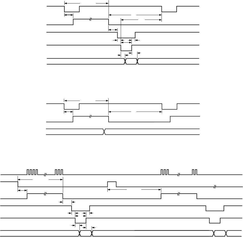
The parallel interfaces of the AD7470 and AD7472 are 10 bits
and 12 bits wide, respectively. The output data buffers are acti-
vated when both CS and RD are logic low. At this point, the con-
tents of the data register are placed onto the data bus. Figure 10
shows the timing diagram for the parallel port.
Figure 11 shows the timing diagram for the parallel port when
CS and RD are tied permanently low. In this setup, once BUSY
line goes from high to low, the conversion process is completed.
The data is available on the output bus slightly before the falling
edge of BUSY.
It is important to point out that data bus cannot change state
while the ADC is doing a conversion as this would have a detri-
mental effect on the conversion in progress. The data out lines
will go three-state again when either the RD or the CS line goes
high. Thus the CS can be tied low permanently, leaving the RD
line to control conversion result access. Refer to V
DRIVE
section
for output voltage levels.
t
2
t
CONVERT
t
3
t
4
t
8
t
5
t
6
t
7
t
9
t
10
BUSY
CS
RD
DBx
CONVST*
*CONVST SHOULD GO HIGH WHEN THE CLK IS HIGH OR BEFORE THE FIRST CLK CYCLE.
Figure 10. Parallel Port Timing
t
2
t
CONVERT
t
9
CONVST*
BUSY
DBx
DATA N DATA N + 1
*CONVST SHOULD GO HIGH WHEN THE CLK IS HIGH OR BEFORE THE FIRST CLK CYCLE.
Figure 11. Parallel Port Timing with
CS
and
RD
Tied Low
t
2
t
3
t
4
t
8
t
6
t
7
CLK IN
CONVST
BUSY
CS
RD
DB
X
t
WAKEUP
t
5
t
CONVERT
Figure 12. Wake-Up Timing Diagram (Burst Clock)

AD7472ARUZ

Mfr. #:
Manufacturer:
Analog Devices Inc.
Description:
Analog to Digital Converters - ADC 12-Bit 2.7V-5.25V 1.5MSPS Lo Pwr
Lifecycle:
New from this manufacturer.
Delivery:
DHL FedEx Ups TNT EMS
Payment:
T/T Paypal Visa MoneyGram Western Union