REV. B
AD7470/AD7472
–13–
OPERATING MODES
The AD7470 and AD7472 have two possible modes of opera-
tion, depending on the state of the CONVST pulse at the end of
a conversion, Mode 1 and Mode 2. There is a continuous clock
on the CLKIN pin.
Mode 1 (High Speed Sampling)
In this mode of operation, the CONVST pulse is brought high
before the end of conversion i.e., before BUSY goes low (see
Figure 10). If the CONVST pin is brought from high to low
while BUSY is high, the conversion is restarted. When operat-
ing in this mode, a new conversion should not be initiated until
the acquisition time has elapsed after BUSY goes low. This
acquisition time allows the track-and-hold circuit to accurately
acquire the input signal. As mentioned earlier, a read should
not be done during a conversion. This mode facilitates the
fastest throughput times for the AD7470/AD7472.
Mode 2 (Sleep Mode)
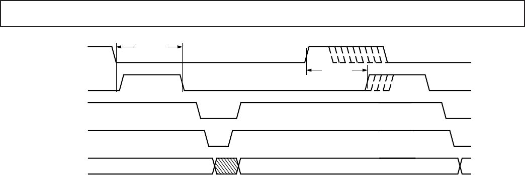
Figure 13 shows AD7470/AD7472 in Mode 2 operation where
the ADC goes into sleep mode after conversion. The CONVST
line is brought low to initiate a conversion and remains low until
after the end of conversion. If CONVST goes high and low
again while BUSY is high, the conversion is restarted. Once the
BUSY line goes from a high to a low, the CONVST line has its
status checked and, if low, the part enters sleep mode.
The device wakes up again on the rising edge of the CONVST
signal. There is a wake-up time of typically 1 µs after the rising
edge of CONVST before the BUSY line can go high to indicate
start of conversion. BUSY will only go high once CONVST goes
low. The CONVST line can go from a high to a low during this
wake-up time, but the conversion will still not be initiated until
after the 1 µs wake-up time. Superior power performance can be
achieved in this mode of operation by waking up the AD7470
and AD7472 only to carry out a conversion.
Burst Mode
Burst mode on the AD7470/AD7472 is a subsection of Mode 1
and Mode 2; the clock is noncontinuous. Figure 12 shows how
the ADC works in burst mode for Mode 2. The clock needs to
be switched on only during conversion, a minimum of 12 clock
cycles for the AD7470 and 14 clock cycles for the AD7472.
Because the clock is off during nonconverting intervals, system
power is saved. The BUSY signal can be used to gate the CLKIN
pulses. The ADC does not begin the conversion process until
CONVST
BUSY
CS
RD
DBx
t
WAKEUP
t
CONVERT
Figure 13. Mode 2 Operation
the first CLKIN rising edge after BUSY goes high. The clock
needs to start less than two clock cycles away from the
CONVST active edge, otherwise INL deteriorates. For
example, if the clock frequency is 28 MHz, the clock must start
within 71.4 ns of CONVST going low. In Figure 12, the A/D
converter section is put into sleep mode once conversion is
completed. On the rising edge of CONVST, it is woken up
again. The user must be wary of the wake-up time because it
will reduce the sampling rate of the ADC.
V
DRIVE
The V
DRIVE
pin is used as the voltage supply to the output driv-
ers and is a separate supply from AV
DD
and DV
DD
. The purpose
of using a separate supply for the output drivers is that the user
can vary the output high voltage, V
OH
, from the V
DD
supply to
the AD7470/AD7472. For example, if AV
DD
and DV
DD
is using
a 5 V supply, the V
DRIVE
pin can be powered from a 3 V supply.
The ADC has better dynamic performance at 5 V than at 3 V,
so operating the part at 5 V, while still being able to interface to
3 V parts, pushes the AD7470/AD7472 to the top bracket of
high performance 10-bit/12-bit ADCs. Of course, the ADC can
have its V
DRIVE
and DV
DD
pins connected together and be pow-
ered from a 3 V or 5 V supply.
All outputs are powered from V
DRIVE
. These are all the data out
pins and the BUSY pin. The CONVST, CS, RD, and CLKIN
signals are related to the DV
DD
voltage.
POWER-UP
It is recommended that the user perform a dummy conversion
after power-up, because the first conversion result could be
incorrect. This also ensures that the part is in the correct mode
of operation. The recommended power-up sequence is as
follows:
1. GND 4. Digital Inputs
2. V
DD
5. REF IN
3. V
DRIVE
6. V
IN
Power vs. Throughput
The two modes of operation for the AD7470 and AD7472 will
produce different power versus throughput performances,
Mode 1 and Mode 2; see Operating Modes section of the data
sheet for more detailed descriptions of these modes. Mode 2 is
the sleep mode of the part and it achieves the optimum power
performance.