REV. B
–4–
AD7470/AD7472
AD7472–SPECIFICATIONS
1
(V
DD
= 2.7 V to 5.25 V
2
, REF IN = 2.5 V,Y Version: f
CLKIN
= 20 MHz @ 5 V and
14 MHz @ 3 V; T
A
= T
MIN
to T
MAX
, unless otherwise noted.)
Parameter Y Version
1
Unit Test Conditions/Comments
DYNAMIC PERFORMANCE 5 V 3 V f
S
= 1.2 MSPS @ 5 V, f
S
= 875 kSPS @ 3 V
Signal to Noise + Distortion (SINAD) 69 69 dB typ f
IN
= 500 kHz Sine Wave
68 68 dB min f
IN
= 100 kHz Sine Wave
Signal-to-Noise Ratio (SNR) 70 70 dB typ f
IN
= 500 kHz Sine Wave
68 68 dB min f
IN
= 100 kHz Sine Wave
Total Harmonic Distortion (THD) –83 –78 dB typ f
IN
= 500 kHz Sine Wave
–83 –84 dB typ f
IN
= 100 kHz Sine Wave
–75 –75 dB max f
IN
= 100 kHz Sine Wave
Peak Harmonic or Spurious Noise (SFDR) –86 81 dB typ f
IN
= 500 kHz Sine Wave
–86 –86 dB typ f
IN
= 100 kHz Sine Wave
–76 –76 dB max f
IN
= 100 kHz Sine Wave
Intermodulation Distortion (IMD)
Second-Order Terms –77 –77 dB typ f
IN
= 500 kHz Sine Wave
–86 –86 dB typ f
IN
= 100 kHz Sine Wave
Third-Order Terms –77 –77 dB typ f
IN
= 500 kHz Sine Wave
–86 –86 dB typ f
IN
= 100 kHz Sine Wave
Aperture Delay 5 5 ns typ
Aperture Jitter 15 15 ps typ
Full Power Bandwidth 20 20 MHz typ @ 3 dB
DC ACCURACY f
S
= 1.2 MSPS @ 5 V; f
S
= 875 kSPS @ 3 V
Resolution 12 12 Bits
Integral Nonlinearity ± 2 ± 2 LSB max
Differential Nonlinearity ± 1.8 ± 1.8 LSB max Guaranteed No Missed Codes to 11 Bits
Offset Error ± 10 ± 10 LSB max
Gain Error ± 2 ± 2 LSB max
ANALOG INPUT
Input Voltage Ranges 0 to REF IN 0 to REF IN V
DC Leakage Current ± 1 ± 1 µA max
Input Capacitance 33 33 pF typ
REFERENCE INPUT
REF IN Input Voltage Range 2.5 2.5 V ±1% for Specified Performance
DC Leakage Current ± 1 ± 1 µA max
Input Capacitance 10/20 10/20 pF typ Track-and-Hold Mode
LOGIC INPUTS
Input High Voltage, V
INH
2.4 2.4 V min
Input Low Voltage, V
INL
0.4 0.4 V max
Input Current, I
IN
± 1 ± 1 µA max Typically 10 nA, V
IN
= 0 V or V
DD
Input Capacitance, C
IN
3
10 10 pF max
LOGIC OUTPUTS
Output High Voltage, V
OH
V
DRIVE
0.2 V
DRIVE
0.2 V min I
SOURCE
= 200 µA
Output Low Voltage, V
OL
0.4 0.4 V max I
SINK
= 200 µA
Floating-State Leakage Current ± 10 ± 10 µA max V
DD
= 2.7 V to 5.25 V
Floating-State Output Capacitance 10 10 pF max
Output Coding Straight (Natural) Binary
CONVERSION RATE
Conversion Time 14 14 CLK IN Cycles (max)
Track-and-Hold Acquisition Time 140 140 ns min
Throughput Rate 1200 875 kSPS max Conversion Time + Acquisition Time
POWER REQUIREMENTS
V
DD
+2.7/+5.25 V min/max
I
DD
4
Digital Inputs = 0 V or DV
DD
Normal Mode 2.4 mA max V
DD
= 4.75 V to 5.25 V; f
S
= 1.2 MSPS; Typ 2 mA
Quiescent Current 900 µA max V
DD
= 4.75 V to 5.25 V; f
S
= 1.2 MSPS
Normal Mode 1.5 mA max V
DD
= 2.7 V to 3.3 V; f
S
= 875 kSPS; Typ 1.3 mA
Quiescent Current 800 µA max V
DD
= 2.7 V to 3.3 V; f
S
= 875 kSPS
Sleep Mode 2 µA max CLK IN = 0 V or DV
DD
Power Dissipation
4
Digital Inputs = 0 V or DV
DD
Normal Mode 12 mW max V
DD
= 5 V
4.5 mW max V
DD
= 3 V
Sleep Mode 10 µW max V
DD
= 5 V; CLK IN = 0 V or DV
DD
6 µW max V
DD
= 3 V; CLK IN = 0 V or DV
DD
NOTES
1
Temperature ranges as follows: Y Version: –40°C to +125°C.
2
The AD7472 functionally works at 2.35 V. Typical specifications @ 25°C for SNR (100 kHz) = 68 dB; THD (100 kHz) = –84 dB; INL ± 0.8 LSB.
3
Sample tested @ 25°C to ensure compliance.
4
See Power vs. Throughput Rate section.
Specifications subject to change without notice.
REV. B
–5–
AD7470/AD7472
Limit at T
MIN
, T
MAX
Parameter AD7470 AD7472 Unit Description
f
CLK
2
10 10 kHz min
30 26 MHz max
t
CONVERT
436.42 531.66 ns min t
CLK
= 1/f
CLK IN
t
WAKEUP
11µs max Wake-Up Time
t
1
10 10 ns min CONVST Pulse Width
t
2
CONVST to BUSY Delay,
10 10 ns max V
DD
= 5 V, A and B Versions
15 ns max V
DD
= 5 V, Y Version
30 30 ns max V
DD
= 3 V, A and B Versions
35 ns max V
DD
= 3 V, Y Version
t
3
00ns max BUSY to CS Setup Time
t
4
3
00ns max CS to RD Setup Time
t
5
20 20 ns min RD Pulse Width
t
6
3
15 15 ns min Data Access Time After Falling Edge of RD
t
7
4
88ns max Bus Relinquish Time After Rising Edge of RD
t
8
00ns max CS to RD Hold Time
t
9
Acquisition Time
135 135 ns max A and B Versions
140 ns max Y Version
t
10
100 100 ns min Quiet Time
NOTES
1
Sample tested at 25°C to ensure compliance. All input signals are specified with tr = tf = 5 ns (10% to 90% of V
DD
) and timed from a voltage level of 1.6 V.
See Figure 1.
2
Mark/Space ratio for the CLK inputs is 40/60 to 60/40. First CLK pulse should be 10 ns min from falling edge of CONVST .
3
Measured with the load circuit of Figure 1 and defined as the time required for the output to cross 0.8 V or 2.0 V.
4
t
7
is derived from the measured time taken by the data outputs to change 0.5 V when loaded with the circuit of Figure 1. The measured number is then extrapolated
back to remove the effects of charging or discharging the 50 pF capacitor. This means that the time, t
7
, quoted in the timing characteristics, is the true bus relinquish
time of the part and is independent of the bus loading.
Specifications subject to change without notice.
TIMING SPECIFICATIONS
1
(V
DD
= 2.7 V to 5.25 V, REF IN = 2.5 V; T
A
= T
MIN
to T
MAX
, unless otherwise noted.)
200A
I
OL
200A
I
OH
C
L
50pF
TO OUTPUT
PIN
1.6V
Figure 1. Load Circuit for Digital Output Timing Specifications
REV. B
AD7470/AD7472
–6–
ORDERING GUIDE
Temperature Resolution Package Package
Model Range (Bits) Options
1
Description
AD7470ARU –40°C to +85°C10 RU-24 TSSOP
AD7470ARU-REEL –40°C to +85°C10 RU-24 TSSOP
AD7470ARU-REEL7 –40°C to +85°C10 RU-24 TSSOP
AD7472AR –40°C to +85°C12 R-24 SOIC
AD7472AR-REEL –40°C to +85°C12 R-24 SOIC
AD7472AR-REEL7 –40°C to +85°C12 R-24 SOIC
AD7472ARU –40°C to +85°C12 RU-24 TSSOP
AD7472ARU-REEL –40°C to +85°C12 RU-24 TSSOP
AD7472ARU-REEL7 –40°C to +85°C12 RU-24 TSSOP
AD7472BR –40°C to +85°C12 R-24 SOIC
AD7472BR-REEL –40°C to +85°C12 R-24 SOIC
AD7472BRU –40°C to +85°C12 RU-24 TSSOP
AD7472BRU-REEL –40°C to +85°C12 RU-24 TSSOP
AD7472BRU-REEL7 –40°C to +85°C12 RU-24 TSSOP
AD7472YR –40°C to +125°C12 R-24 SOIC
AD7472YR-REEL –40°C to +125°C12 R-24 SOIC
AD7472YRU –40°C to +125°C12 RU-24 TSSOP
AD7472YRU-REEL –40°C to +125°C12 RU-24 TSSOP
AD7472YRU-REEL7 –40°C to +125°C12 RU-24 TSSOP
EVAL-AD7470CB
2
Evaluation Board
EVAL-AD7472CB
2
Evaluation Board
EVAL CONTROL BRD2
3
Controller Board
NOTES
1
R = SOIC; RU = TSSOP.
2
This can be used as a standalone evaluation board or in conjunction with the EVAL-CONTROL BOARD for evaluation/demonstration purposes.
3
This board is a complete unit allowing a PC to control and communicate with all Analog Devices evaluation boards ending in the CB designators.
To order a complete evaluation kit, you need to order the specific ADC evaluation board, for example, EVAL-AD7472CB, the EVAL CONTROL
BRD2, and a 12 V ac transformer. See the relevant evaluation board application note for more information.
ABSOLUTE MAXIMUM RATINGS
1
(T
A
= 25°C unless otherwise noted.)
AV
DD
to AGND/DGND . . . . . . . . . . . . . . . . . –0.3 V to +7 V
DV
DD
to AGND/DGND . . . . . . . . . . . . . . . . . –0.3 V to +7 V
V
DRIVE
to AGND/DGND . . . . . . . . . . . . . . . . –0.3 V to +7 V
AV
DD
to DV
DD
. . . . . . . . . . . . . . . . . . . . . . –0.3 V to +0.3 V
V
DRIVE
to DV
DD
. . . . . . . . . . . . . . . –0.3 V to DV
DD
+ 0.3 V
AGND to DGND . . . . . . . . . . . . . . . . . . . . –0.3 V to +0.3 V
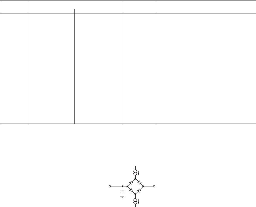
Analog Input Voltage to AGND . . . . –0.3 V to AV
DD
+ 0.3 V
Digital Input Voltage to DGND . . . . –0.3 V to DV
DD
+ 0.3 V
REF IN to AGND . . . . . . . . . . . . . . . –0.3 V to AV
DD
+ 0.3 V
Input Current to Any Pin Except Supplies
2
. . . . . . . . ± 10 mA
Operating Temperature Range
Commercial (A and B Versions) . . . . . . . . . –40°C to +85°C
Industrial (Y Version) . . . . . . . . . . . . . . . –40°C to +125°C
Storage Temperature Range . . . . . . . . . . . –65°C to +150°C
CAUTION
ESD (electrostatic discharge) sensitive device. Electrostatic charges as high as 4000 V readily
accumulate on the human body and test equipment and can discharge without detection.
Although the AD7470/AD7472 features proprietary ESD protection circuitry, permanent dam-
age may occur on devices subjected to high energy electrostatic discharges. Therefore, proper
ESD precautions are recommended to avoid performance degradation or loss of functionality.
Junction Temperature . . . . . . . . . . . . . . . . . . . . . . . . . 150°C
θ
JA
Thermal Impedance . . . . . . . . . . . . . . . 75°C/W (SOIC)
. . . . . . . . . . . . . . . . . . . . . . . . . . . . . . . . .115°C/W (TSSOP)
θ
JC
Thermal Impedance . . . . . . . . . . . . . . . 25°C/W (SOIC)
. . . . . . . . . . . . . . . . . . . . . . . . . . . . . . . . 35°C/W (TSSOP)
Lead Temperature, Soldering
Vapor Phase (60 sec) . . . . . . . . . . . . . . . . . . . . . . . . 215°C
Infrared (15 sec) . . . . . . . . . . . . . . . . . . . . . . . . . . . . 220°C
ESD . . . . . . . . . . . . . . . . . . . . . . . . . . . . . . . . . . . . . . . .1.5 kV
NOTES
1
Stresses above those listed under Absolute Maximum Ratings may cause perma-
nent damage to the device. This is a stress rating only; functional operation of the
device at these or any other conditions above those listed in the operational
sections of this specification is not implied. Exposure to absolute maximum rating
conditions for extended periods may affect device reliability.
2
Transient currents of up to 100 mA will not cause SCR latch-up.

AD7472ARUZ

Mfr. #:
Manufacturer:
Analog Devices Inc.
Description:
Analog to Digital Converters - ADC 12-Bit 2.7V-5.25V 1.5MSPS Lo Pwr
Lifecycle:
New from this manufacturer.
Delivery:
DHL FedEx Ups TNT EMS
Payment:
T/T Paypal Visa MoneyGram Western Union