REV. D
AD641
–9–
Note that this lower limit is not determined by the intercept
voltage, V
X
; it can occur either above or below V
X
, depending
on the design. When using two AD641s in cascade, input offset
voltage and wideband noise are the major limitations to low
level accuracy. Offset can be eliminated in various ways. Noise
can only be reduced by lowering the system bandwidth, using a
filter between the two devices.
EFFECT OF WAVEFORM ON INTERCEPT
The absolute value response of the AD641 allows inputs of
either polarity to be accepted. Thus, the logarithmic output in
response to an amplitude-symmetric square wave is a steady
value. For a sinusoidal input the fluctuating output current will
usually be low-pass filtered to extract the baseband signal. The
unfiltered output is at twice the carrier frequency, simplifying the
design of this filter when the video bandwidth must be maxi-
mized. The averaged output depends on waveform in a roughly
analogous way to waveform dependence of rms value. The effect
is to change the apparent intercept voltage. The intercept volt-
age appears to be doubled for a sinusoidal input, that is, the
averaged output in response to a sine wave of amplitude (not rms
value) of 20 mV would be the same as for a dc or square wave
input of 10 mV. Other waveforms will result in different inter-
cept factors. An amplitude-symmetric-rectangular waveform has
the same intercept as a dc input, while the average of a base-
band unipolar pulse can be determined by multiplying the
response to a dc input of the same amplitude by the duty cycle.
It is important to understand that in responding to pulsed RF
signals it is the waveform of the carrier (usually sinusoidal) not
the modulation envelope, that determines the effective intercept
voltage. Table I shows the effective intercept and resulting deci-
bel offset for commonly occurring waveforms. The input wave-
form does not affect the slope of the transfer function. Figure 22
shows the absolute deviation from the ideal response of cascaded
AD641s for three common waveforms at input levels from
–80 dBV to –10 dBV. The measured sine wave and triwave
responses are 6 dB and 8.7 dB, respectively, below the square
wave response—in agreement with theory.
Table I.
Input Peak Intercept Error (Relative
Waveform or rms Factor to a DC Input)
Square Wave Either 1 0.00 dB
Sine Wave Peak 2 –6.02 dB
Sine Wave rms 1.414 (2) –3.01 dB
Triwave Peak 2.718 (e) –8.68 dB
Triwave rms 1.569 (e/3) –3.91 dB
Gaussian Noise rms 1.887 –5.52 dB
Logarithmic Conformance and Waveform
The waveform also affects the ripple, or periodic deviation from
an ideal logarithmic response. The ripple is greatest for dc or
square wave inputs because every value of the input voltage
maps to a single location on the transfer function and thus traces
out the full nonlinearities in the logarithmic response.
2
0
–2
–4
–6
–8
–10
–70 –60 –50 –40 –30 –20 –10–80
INPUT AMPLITUDE IN dB ABOVE 1V, AT 10kHz
SQUARE
WAVE INPUT
SINE WAVE
INPUT
TRIWAVE
INPUT
DEVIATION FROM EXACT LOGARITHMIC
TRANSFER FUNCTION – dB
Figure 22. Deviation from Exact Logarithmic Transfer
Function for Two Cascaded AD641s, Showing Effect of
Waveform on Calibration and Linearity
By contrast, a general time varying signal has a continuum of
values within each cycle of its waveform. The averaged output is
thereby “smoothed” because the periodic deviations away from
the ideal response, as the waveform “sweeps over” the transfer
function, tend to cancel. This smoothing effect is greatest for a
triwave input, as demonstrated in Figure 22.
The accuracy at low signal inputs is also waveform dependent.
The detectors are not perfect absolute value circuits, having a
sharp “corner” near zero; in fact they become parabolic at low
levels and behave as if there were a dead zone. Consequently,
the output tends to be higher than ideal. When there are enough
stages in the system, as when two AD641s are connected in
cascade, most detectors will be adequately loaded due to the
high overall gain, but a single AD641 does not have sufficient
gain to maintain high accuracy for low level sine wave or triwave
inputs. Figure 23 shows the absolute deviation from calibration
for the same three waveforms for a single AD641. For inputs
between –10 dBV and –40 dBV the vertical displacement of the
traces for the various waveforms remains in agreement with the
predicted dependence, but significant calibration errors arise at
low signal levels.
4
2
0
–2
–4
–6
–8
–10
–70
INPUT AMPLITUDE IN dB ABOVE 1V, AT 10kHz
–60 –50 –40 –30 –20 –10
–12
DEVIATION FROM EXACT LOGARITHMIC
TRANSFER FUNCTION – dB
SQUARE
WAVE INPUT
SINE WAVE
INPUT
TRIWAVE
INPUT
Figure 23. Deviation from Exact Logarithmic Transfer
Function for a Single AD641, Compare Low Level
Response with That of Figure 22
REV. D
AD641
–10–
SIGNAL MAGNITUDE
The AD641 is a calibrated device. It is, therefore, important to
be clear in specifying the signal magnitude under all waveform
conditions. For dc or square wave inputs there is, of course, no
ambiguity. Bounded periodic signals, such as sinusoids and
triwaves, can be specified in terms of their simple amplitude
(peak value) or alternatively by their rms value (which is a mea-
sure of power when the impedance is specified). It is generally bet-
ter to define this type of signal in terms of its amplitude because
the AD641 response is a consequence of the input voltage, not
power. However, provided that the appropriate value of inter-
cept for a specific waveform is observed, rms measures may be
used. Random waveforms can only be specified in terms of rms
value because their peak value may be unbounded, as is the case
for Gaussian noise. These must be treated on a case-by-case
basis. The effective intercept given in Table I should be used for
Gaussian noise inputs.
On the other hand, for bounded signals the amplitude can be
expressed either in volts or dBV (decibels relative to 1 V). For
example, a sine wave or triwave of 1 mV amplitude can also be
defined as an input of –60 dBV, one of 100 mV amplitude as
–20 dBV, and so on. RMS value is usually expressed in dBm
(decibels above 1 mW) for a specified impedance level. Through-
out this data sheet we assume a 50
environment, the customary
impedance level for high speed systems, when referring to signal pow-
ers in dBm. Bearing in mind the above discussion of the effect of
waveform on the intercept calibration of the AD641, it will be
apparent that a sine wave at a power of, say, –10 dBm will not
produce the same output as a triwave or square wave of the
same power. Thus, a sine wave at a power level of –10 dBm has
an rms value of 70.7 mV or an amplitude of 100 mV (that is, 2
times as large, the ratio of amplitude to rms value for a sine
wave), while a triwave of the same power has an amplitude
which is 3 or 1.73 times its rms value, or 122.5 mV.
“Intercept” and “Logarithmic Offset”
If the signals are expressed in dBV, we can write the output
current in a simpler form, as:
I
OUT
= 50
µ
A (Input
dBV
– X
dBV
) Equation (4)
where Input
dBV
is the input voltage amplitude (not rms) in dBV
and X
dBV
is the appropriate value of the intercept (for a given wave-
form) in dBV. This form shows more clearly why the intercept is
often referred to as the logarithmic offset. For dc or square wave
inputs, V
X
is 1 mV so the numerical value of X
dBV
is –60, and
Equation (4) becomes
I
OUT
= 50
µ
A (Input
dBV
+ 60) Equation (5)
Alternatively, for a sinusoidal input measured in dBm (power in
dB above 1 mW in a 50 system) the output can be written
I
OUT
= 50
µ
A (Input
dBm
+ 44) Equation (6)
because the intercept for a sine wave expressed in volts rms is at
1.414 mV (from Table I) or –44 dBm.
OPERATION OF A SINGLE AD641
Figure 24 shows the basic connections for a single device, using
100 load resistors. Output A is a negative going voltage with a
slope of –100 mV per decade; output B is positive going with a
slope of +100 mV per decade. For applications where absolute
calibration of the intercept is essential, the main output (from
LOG OUT, Pin 14) should be used; the LOG COM output can
then be grounded. To evaluate the demodulation response, a
simple low pass output filter having a time constant of roughly
500 µs (3 dB corner of 320 Hz) is provided by a 4.7 µF (–20%
+80%) ceramic capacitor (Erie type RPE117-Z5U-475-K50V)
placed across the load. A DVM may be used to measure the
averaged output in verification tests. The voltage compliance at
Pins 13 and 14 extends from 0.3 V below ground up to 1 V
below +V
S
. Since the current into Pin 14 is from –0.2 mA at
zero signal to +2.3 mA when fully limited (dc input of >300 mV)
the output never drops below –230 mV. On the other hand, the
current out of Pin 13 ranges from –0.2 mA to +2.3 mA, and if
desired, a load resistor of up to 2 k can be used on this output;
the slope would then be 2 V per decade. Use of the LOG COM
output in this way provides a numerically correct decibel read-
ing on a DVM (+100 mV = +1.00 dB).
Board layout is very important. The AD641 has both high gain
and wide bandwidth; therefore every signal path must be very
carefully considered. A high quality ground plane is essential,
but it should not be assumed that it behaves as an equipotential
plane. Even though the application may only call for modest
bandwidth, each of the three differential signal interface pairs
(SIG IN, Pins l and 20, SIG OUT, Pins 10 and 11, and LOG,
Pins 13 and 14) must have their own “starred” ground points to
avoid oscillation at low signal levels (where the gain is highest).
OUTPUT A
10V
11
DENOTES A SHORT, DIRECT CONNECTION
TO THE GROUND PLANE.
16181920 17
9
8
76
10
53214
LOG
OUT
LOG
COM
SIG
+OUT
RG2
–V
S
SIG
–OUT
AD641
RG0RG1CKT
COM
ATN
OUT
SIG
+IN
+V
S
ITCBL1
ATN
IN
ATN
COM
ATN
COM
ATN
LO
SIG
–IN
BL2
1kV
1kV
NC NC
4.7V
–5V
NC
ALL UNMARKED CAPACITORS ARE
0.1mF CERAMIC (SEE TEXT).
OUTPUT B
4.7mF
R
LA
100V
0.1%
R
LB
+5V
OPTIONAL
OFFSET BALANCE
RESISTOR
OPTIONAL
TERMINATION
RESISTOR
SIGNAL
INPUT
12
13
1415
4.7mF
100V
0.1%
Figure 24. Connections for a Single AD641 to Verify Basic Performance
REV. D
AD641
–11–
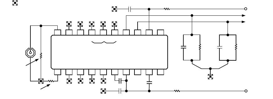
Unused pins (excluding Pins 8, 10 and 11) such as the attenua-
tor and applications resistors should be grounded close to the
package edge. BL1 (Pin 6) and BL2 (Pin 9) are internal bias
lines a volt or two above the –V
S
node; access is provided solely
for the addition of decoupling capacitors, which should be con-
nected exactly as shown (not all of them connect to the ground).
Use low impedance ceramic 0.1 µF capacitors (for example,
Erie RPE113-Z5U-105-K50V). Ferrite beads may be used
instead of supply decoupling resistors in cases where the supply
voltage is low.
Active Current-to-Voltage Conversion
The compliance at LOG OUT limits the available output volt-
age swing. The output of the AD641 may be converted to a
larger, buffered output voltage by the addition of an operational
amplifier connected as a current-to-voltage (transresistance)
stage, as shown in Figure 21. Using a 2 k feedback resistor
(R2) the 50 µA/dB output at LOG OUT is converted to a volt-
age having a slope of +100 mV/dB, that is, 2 V per decade.
This output ranges from roughly –0.4 V for zero signal inputs
to the AD641, crosses zero at a dc input of precisely +1 mV
(or –1 mV) and is +4 V for a dc input of 100 mV. A passive
prefilter, formed by R1 and C1, minimizes the high frequency
energy conveyed to the op amp. The corner frequency is here
shown as 10 MHz. The AD846 is recommended for this appli-
cation because of its excellent performance in transresistance
modes. Its bandwidth of 35 MHz (with the 2 k feedback resis-
tor) will exceed the baseband response of the system in most
applications. For lower bandwidth applications other op amps
and multipole active filters may be substituted.
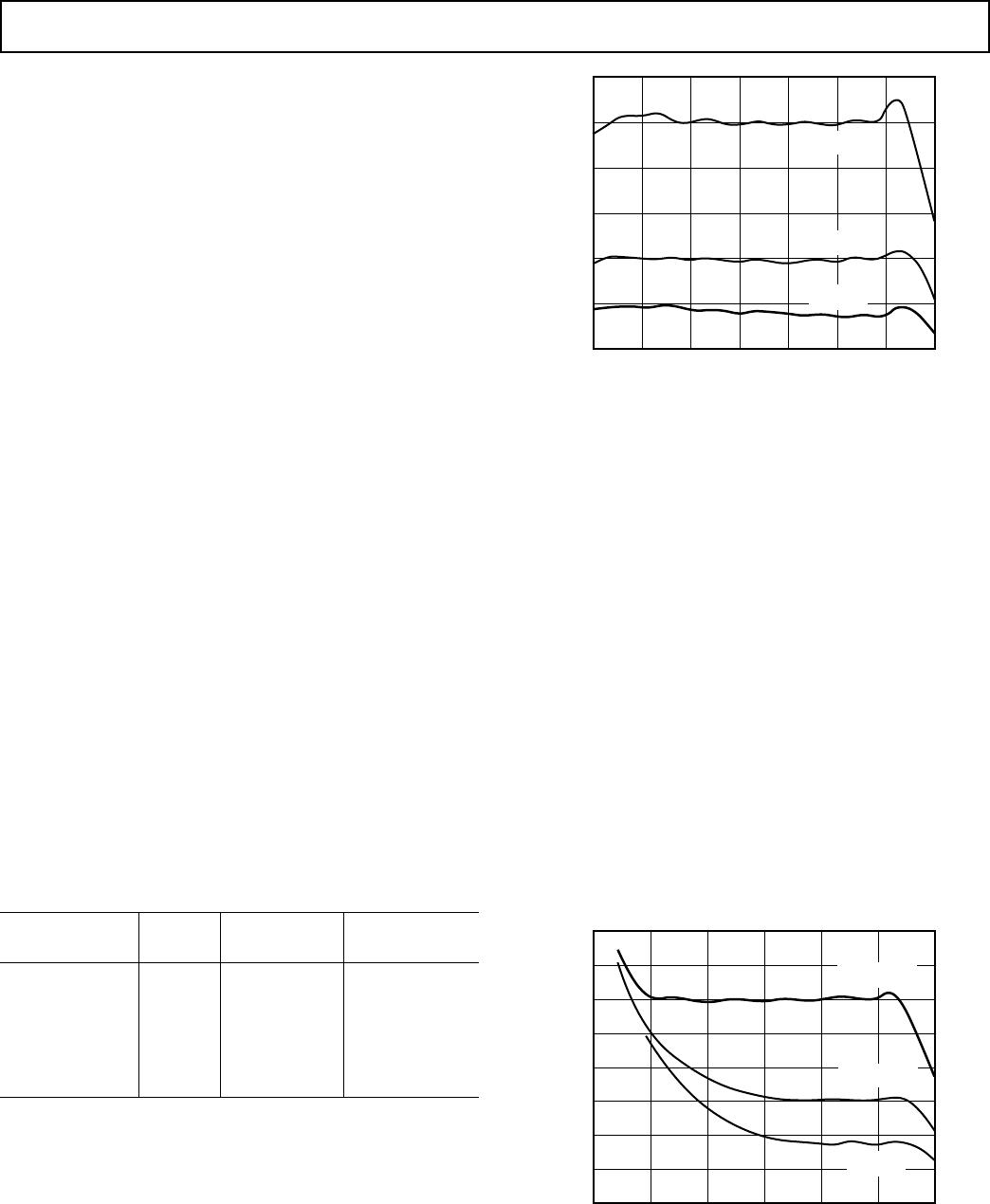
Effect of Frequency on Calibration
The slope and intercept of the AD641 are calibrated during
manufacture using a 2 kHz square wave input. Calibration
depends on the gain of each stage being 10 dB. When the input
frequency is an appreciable fraction of the 350 MHz bandwidth
of the amplifier stages, their gain becomes less precise and the
logarithmic slope and intercept are no longer as calibrated.
Figure 10 shows the averaged output current versus input level
at 50 MHz, 150 MHz, 190 MHz, 210 MHz, and 250 MHz.
Figure 11 shows the absolute error in the response at 200 MHz
and at temperatures of –55°C, +25°C and +125°C. Figure 12
shows the variation in the slope current, and Figure 13 shows
the variation in the intercept level (sinusoidal input) versus
frequency.
If absolute calibration is essential, or some other value of slope
or intercept is required, there will usually be some point in the
user’s system at which an adjustment may be easily introduced.
For example, the 5% slope deficit at 50 MHz (see Figure 12)
may be restored by a 5% increase in the value of the load resis-
tor in the passive loading scheme shown in Figure 24, or by
inserting a trim potentiometer of 100 in series with the feed-
back resistor in the scheme shown in Figure 21. The intercept
can be adjusted by adding or subtracting a small current to the
output. Since the slope current is 1 mA/decade, a 50 µA incre-
ment will move the intercept by 1 dB. Note that any error in
this current will invalidate the calibration of the AD641. For
example, if one of the 5 V supplies were used with a resistor to
generate the current to reposition the intercept by 20 dB, a
±10% variation in this supply will cause a ±2 dB error in the
absolute calibration. Of course, slope calibration is unaffected.
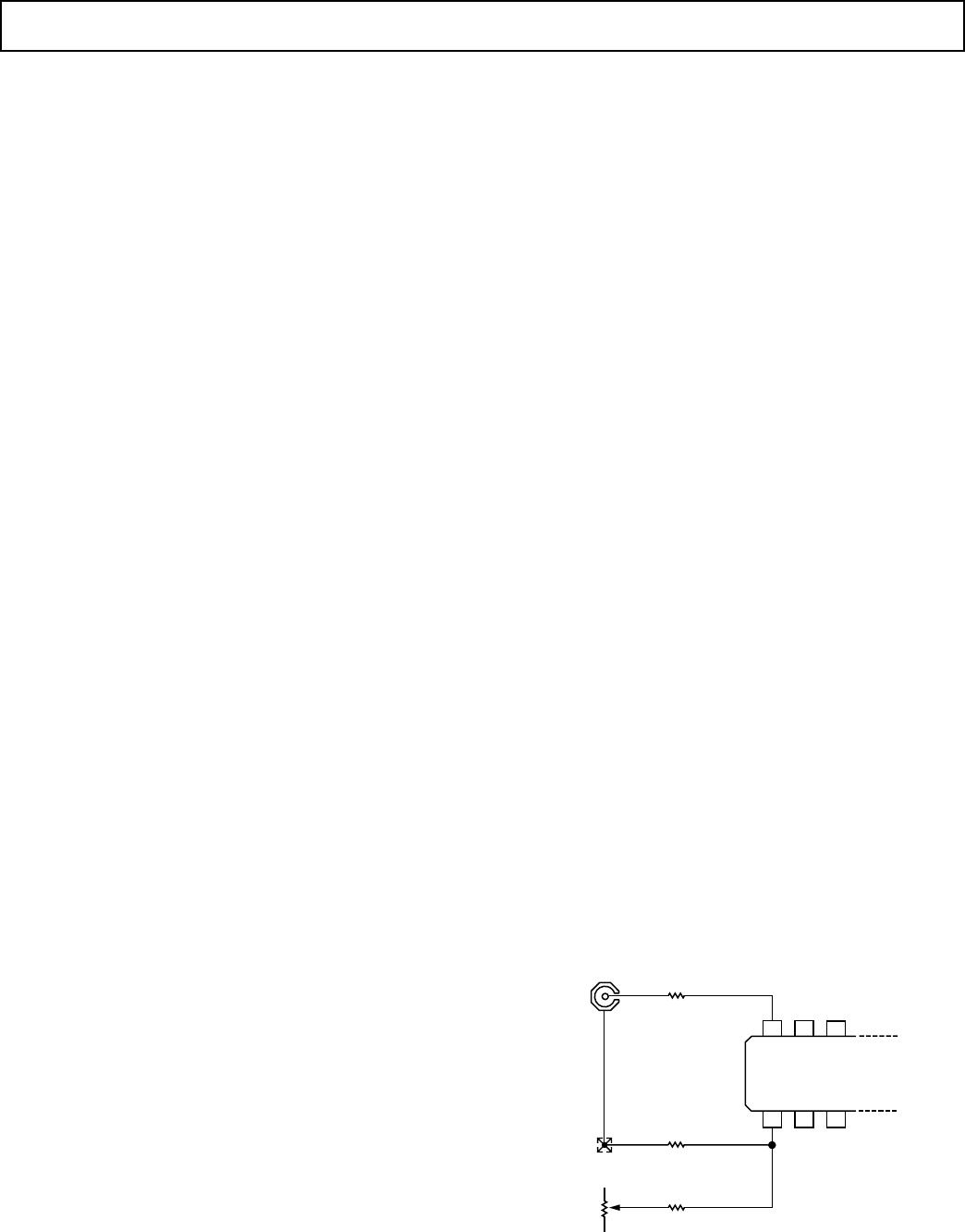
Source Resistance and Input Offset
The bias currents at the signal inputs (Pins 1 and 20) are typi-
cally 7 µA. These flow in the source resistances and generate
input offset voltages which may limit the dynamic range because
the AD641 is direct coupled and an offset is indistinguishable
from a signal. It is good practice to keep the source resistances
as low as possible and to equalize the resistance seen at each
input. For example, if the source resistance to Pin 20 is 100 , a
compensating resistor of 100 should be placed in series with
Pin 1. The residual offset is then due to the bias current offset,
which is typically under 1 µA, causing an extra offset uncertainty
of 100 µV in this example. For a single AD641 this will rarely be
troublesome, but in some applications it may need to be nulled
out, along with the internal voltage offset component. This may
be achieved by adding an adjustable voltage of up to ±250 µV
at the unused input. (Pins 1 and 20 may be interchanged with
no change in function.)
In most applications there will be no need to use any offset
adjustment. However, a general offset trimming circuit is shown
in Figure 25. R
S
is the source resistance of the signal. Note: 50
rf sources may include a blocking capacitor and have no dc path to
ground, or may be transformer coupled and have a near zero resis-
tance to ground. Determine whether the source resistance is zero,
25 or 50 (with the generator terminated in 50 ) to find
the correct value of bias compensating resistor, R
B
, which
should optimally be equal to R
S
, unless R
S
= 0, in which case
use R
B
= 5 . The value of R
OS
should be set to 20,000 R
B
to
provide a ±250 µV trim range. To null the offset, set the source
voltage to zero and use a DVM to observe the logarithmic out-
put voltage. Recall that the LOG OUT current of the AD641
exhibits an absolute value response to the input voltage, so the
offset potentiometer is adjusted to the point where the logarithmic
output “turns around” (reaches a local maximum or minimum).
At high frequencies it may be desirable to insert a coupling
capacitor and use a choke between Pin 20 and ground, when
Pin 1 should be taken directly to ground. Alternatively, trans-
former coupling may be used. In these cases, there is no added
offset due to bias currents. When using two dc-coupled AD641s
(overall gain 100,000), it is impractical to maintain a sufficiently
low offset voltage using a manual nulling scheme. The section
CASCADED OPERATION explains how the offset can be
automatically nulled to submicrovolt levels by the use of a nega-
tive feedback network.
–5V
(SOURCE
RESISTANCE
OF
TERMINATED
GENERATOR)
R
B
2
19
1
20
R
OS
R
S
+5V
20kV
AD641
Figure 25. Optional Input Offset Voltage Nulling Circuit;
See Text for Component Values

AD641ANZ

Mfr. #:
Manufacturer:
Description:
Logarithmic Amplifiers IC 250MHZ DEMOD LGAMP
Lifecycle:
New from this manufacturer.
Delivery:
DHL FedEx Ups TNT EMS
Payment:
T/T Paypal Visa MoneyGram Western Union

Products related to this Datasheet